Integration of a sense fet into a discrete power mosfet

a technology of discrete power and sense fet, which is applied in the direction of semiconductor devices, electrical equipment, transistors, etc., can solve the problems of affecting the performance of the device, and achieve the effect of not greatly affecting the accuracy of the designed sense ratio, affecting the number of main fet cells damaged, and relatively small damage to main fet cells

Active Publication Date: 2009-10-08
ALPHA & OMEGA SEMICON LTD
View PDF7 Cites 34 Cited by
  • Summary
  • Abstract
  • Description
  • Claims
  • Application Information

AI Technical Summary

Benefits of technology

[0013]The gate and source structures that make up the main FET 102 generally lie underneath the main FET source metal 106. The source structures of the sense FET 104 are electrically connected to a sense FET source metal 108. The gate and source structures that make up the sense FET 104 generally lie under a portion of the sense FET source metal 108. However, these structures generally do not lie underneath the sense FET source pad 118 (sometimes referred to as a sense pad) to avoid damage caused by wire bonding impact. Because the number of sense FET cells is usually in orders of magnitude smaller than the number of the main FET cells, such damage to the sense FET cells would greatly affect the accuracy of designed sense ratio. The main FET cells are also exposed to damage from wire bonding impact, but the number of main FET cells damaged is relatively small compared to the total number of main FET cells, so that does not greatly affect the accuracy of the designed sense ratio. The sense FET source metal 108 may cover the whole sense FET source regions and extend to an area without active sense FET cells 104 where the sense pad may be formed directly on the FET source metal 108 or over a passivation layer over the sense FET source metal 108. The passivation layer is not shown in FIG. 1 for the sake of simplicity. FIG. 1A shows the same top view as FIG. 1, but also shows a passivation layer 208 and the windows opened in the passivation layer 208 to allow bonding to the main FET source metal 106, sense FET source metal 108, and outer gate metal 111 according to one embodiment of the invention. The metal exposed by the windows in the passivation layer 208 in effect form the gate pad 120, the main FET source pad 107, and the sense FET source pad 118. It is clear that the sense FET 104 is not located directly under the sense FET source pad 118.
[0022]Multiple Sense FETs with a number of different current ratios may be easily integrated into main power MOSFET. FIG. 3D is showing a semiconductor device 310 including two sense FETs 312 and 314 located proximate corners of the main FET 302. Source metal for the main FET and two sense FETs lies between the FETs and corresponding source pads 311, 313, 315 and a gate pad 317. Gaps 316, 318, 319 are formed in a common metal layer to divide it into a gate metal region and source metal regions for the main FET and each sense FET. The source pads 311, 313, 315 for the main FET and sense FETS overlie the corresponding metal regions. The gate pad 317 overlies a portion of the gate metal region. An electrical isolator 320 indicated by the dashed line may be formed in a body portion of the substrate in a suitable pattern to electrically isolate the source regions of the main FET and sense FETS.

Problems solved by technology

However, the wire bonding between the sense FET and the main FET will affect the performance of the device.

Method used


Image

  • Integration of a sense fet into a discrete power mosfet
  • Integration of a sense fet into a discrete power mosfet
  • Integration of a sense fet into a discrete power mosfet

Examples


Embodiment Construction

[0011]Although the following detailed description contains many specific details for the purposes of illustration, anyone of ordinary skill in the art will appreciate that many variations and alterations to the following details are within the scope of the invention. Accordingly, the exemplary embodiments of the invention described below are set forth without any loss of generality to, and without imposing limitations upon, the claimed invention.

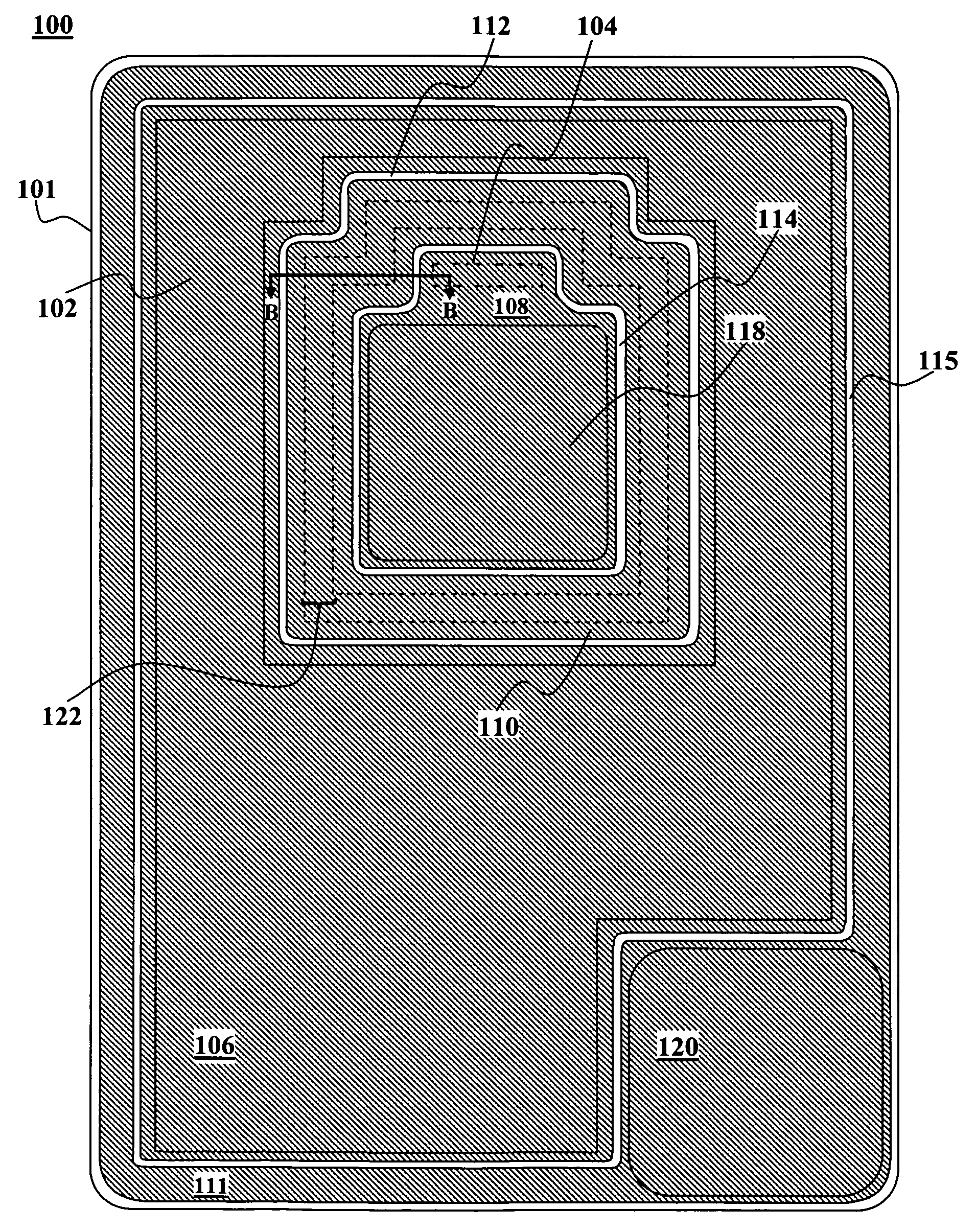
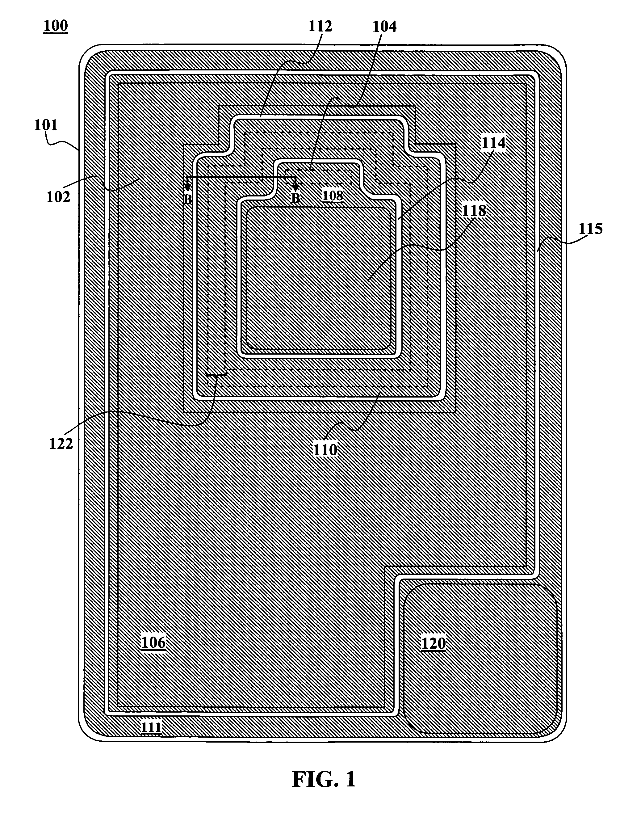
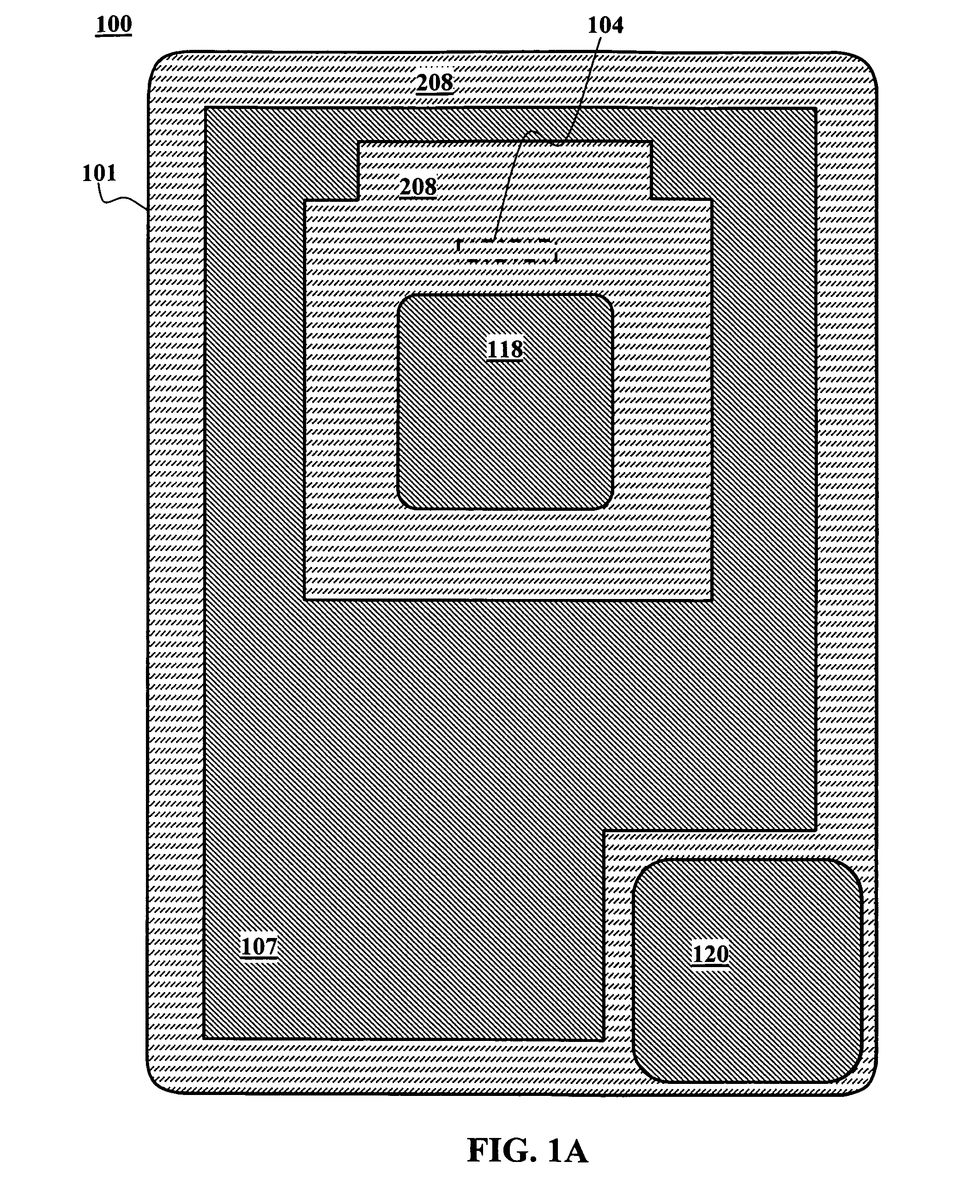
[0012]Certain aspects of embodiments of the invention may be understood by referring simultaneously to FIG. 1, FIG. 1A and FIG. 2. FIG. 1 illustrates a top plan view of a semiconductor device 100 according to an embodiment of the present invention. As shown in FIG. 1, the semiconductor device 100 includes a common substrate 101, a main FET 102, disposed in the common substrate 101, and one or more sense FETs 104, also disposed in the common substrate. As shown in the example depicted in FIG. 1, the sense FET 104 may be built in an area surro...


PUM


Abstract

A semiconductor device includes a main field effect transistor (FET) and one or more sense FETs, and a common gate pad. The main FET and the one or more sense FETs are formed in a common substrate. The main FET and each of the sense FETs include a source terminal, a gate terminal and a drain terminal. The common gate pad connects the gate terminals of the main FET and the one or more sense FETs. An electrical isolation is disposed between the gate terminals of the main FET and the one or more sense FETs. Embodiments of this invention may be applied to both N-channel and P-channel MOSFET devices.

Description

FIELD OF THE INVENTION[0001]Embodiments of this invention generally relate to semiconductor devices and more particularly to semiconductor devices including a power MOSFET and one or more sense MOSFETs with common gate and drain terminals and separate source terminals.BACKGROUND OF THE INVENTION[0002]One method for determining the current through a load in a circuit is to use a metal oxide semiconductor field effect transistor (MOSFET) for current sensing. Current sensing power MOSFETs conventionally include several thousand transistor cells arranged in parallel and sharing common drain, source and gate electrodes. Each transistor cell or element within the device is identical and current applied at the drain terminal of the device is shared equally between them. In such designs, it is common that the source electrodes of several of the transistors are separated from the remaining source electrodes and connected to a separate source terminal. Accordingly, the resulting current sensi...

Claims


Application Information

Patent Timeline
Patent Type & Authority Applications(United States)
IPC IPC(8): H01L27/088H01L21/8232
CPCH01L21/8234H01L27/088H01L29/0646H01L29/0653H01L29/0696H01L29/66734H01L2924/13091H01L29/7813H01L29/7815H01L2224/0603H01L2924/00
Inventor SU, YIBHALLA, ANUPNG, DANIEL
Owner ALPHA & OMEGA SEMICON LTD
Why Eureka
Try Eureka