

Variable capacitance circuit
a capacitance circuit and variable technology, applied in the field of variable capacitance circuits, can solve the problems of large area occupied by resistors ri, unfavorable, and strong reception signals that cannot be handled, and achieve the effect of suppressing distortion of input signals and reducing capacitan
- Summary
- Abstract
- Description
- Claims
- Application Information
AI Technical Summary
Benefits of technology
Problems solved by technology
Method used
Image

Examples
Embodiment Construction
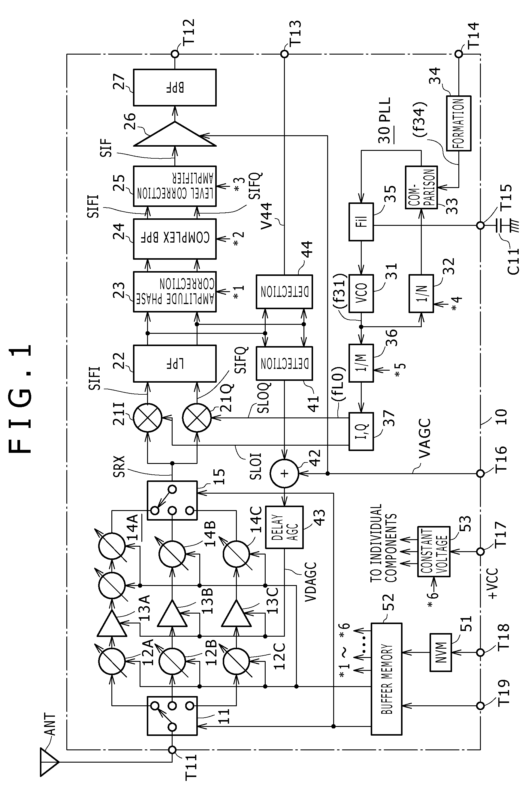
[0033]Here, a television receiver with which a variable capacitance circuit according to the present invention is used suitably is described first.
[0034]Example of the (Entire) Reception Circuit Frequencies (channels) used for television broadcast differ among different countries, and also for the color television system, NTSC, PAL, SECAM and so forth are available. Further, not only analog broadcasts but also digital broadcasts are available.
[0035]Thus, it has been proposed to divide a reception signal system of a television broadcast into a front end circuit which receives a television broadcast and outputs an intermediate frequency signal, and a base-band processing circuit which processes an output of the front end circuit and outputs a color image signal and a sound signal. In short, it is intended to cope with a difference in the broadcasting system of a television broadcast by such countermeasure.
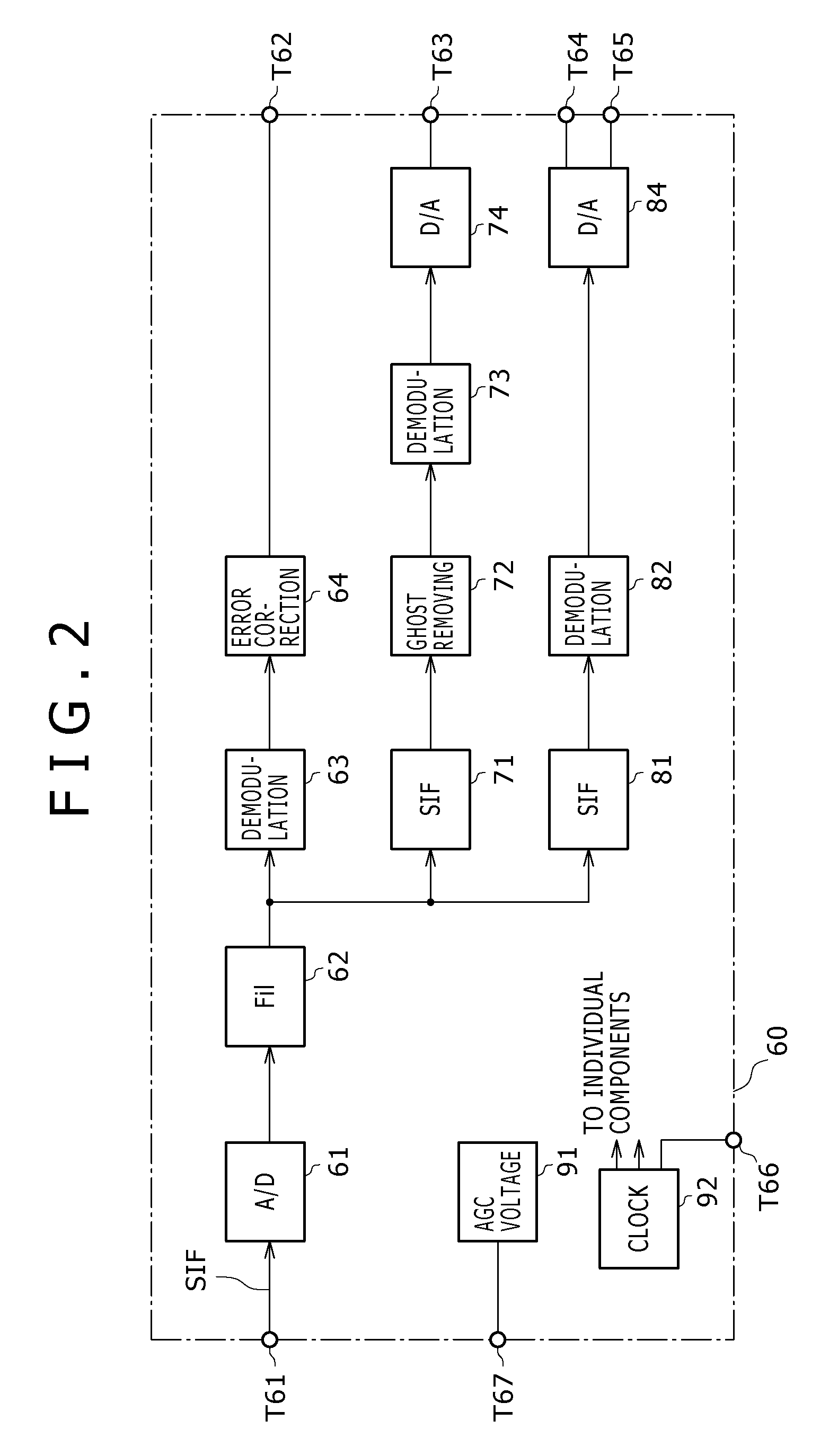
[0036]Therefore, an example of a front end circuit and a base-band processing ci...
PUM
 Abstract
Description
Claims
Application Information