Millimeter-band switching circuit

a switching circuit and millimeter-band technology, applied in the field of millimeter-band switching circuits, can solve the problems of affecting the insertion loss of the capacitor cb, affecting the insertion loss of the switching element, and affecting the insertion characteristic, so as to achieve the effect of easy correction of the varied off capacitance of the switching elemen

Inactive Publication Date: 2009-08-18
MITSUBISHI ELECTRIC CORP
View PDF5 Cites 0 Cited by
  • Summary
  • Abstract
  • Description
  • Claims
  • Application Information

AI Technical Summary

Benefits of technology

[0015]The present invention has been made to solve one of the above-mentioned problems and an object of the present invention is to obtain a millimeter-band switching circuit capable of easily correcting a varied off capacitance of a switching element without shifting a position of the switching element.
[0016]The present invention has been made to solve another one of the above-mentioned problems and another object of the present invention is to obtain a millimeter-band switching circuit capable of suppressing an increase in insertion loss without providing a capacitor in a branch point.
[0017]Further, the present invention has been made to solve another one of the above-mentioned problems and another object of the present invention is to obtain a millimeter-band switching circuit in which the number of parts can be decreased to reduce cost.
[0019]According to the present invention, the millimeter-band switching circuit has an effect that the varied off capacitance of the switching element can be easily corrected without shifting the position of the switching element.

Problems solved by technology

Therefore, there is a problem that the characteristics are shifted to a low-frequency side.
Therefore, there is a problem that the insertion loss is increased by the capacitor C1.
As described above, in the conventional millimeter-band SPST switching circuit, when the off capacitance of the FET (switching element) increases, there is a problem that the insertion loss and the isolation characteristic are shifted to the low-frequency side.
In order to solve such a problem, it is necessary to shorten the line length of the transmission line L4 between the two FETs, which leads to another problem in that the FETs need to be shifted in position.
Therefore, there is a problem that the insertion loss is increased by the capacitor C1.
The conventional millimeter-band switching circuit using the coupling line has a problem that the number of parts is large, thereby increasing cost.

Method used


Image

  • Millimeter-band switching circuit
  • Millimeter-band switching circuit
  • Millimeter-band switching circuit

Examples


embodiment 1

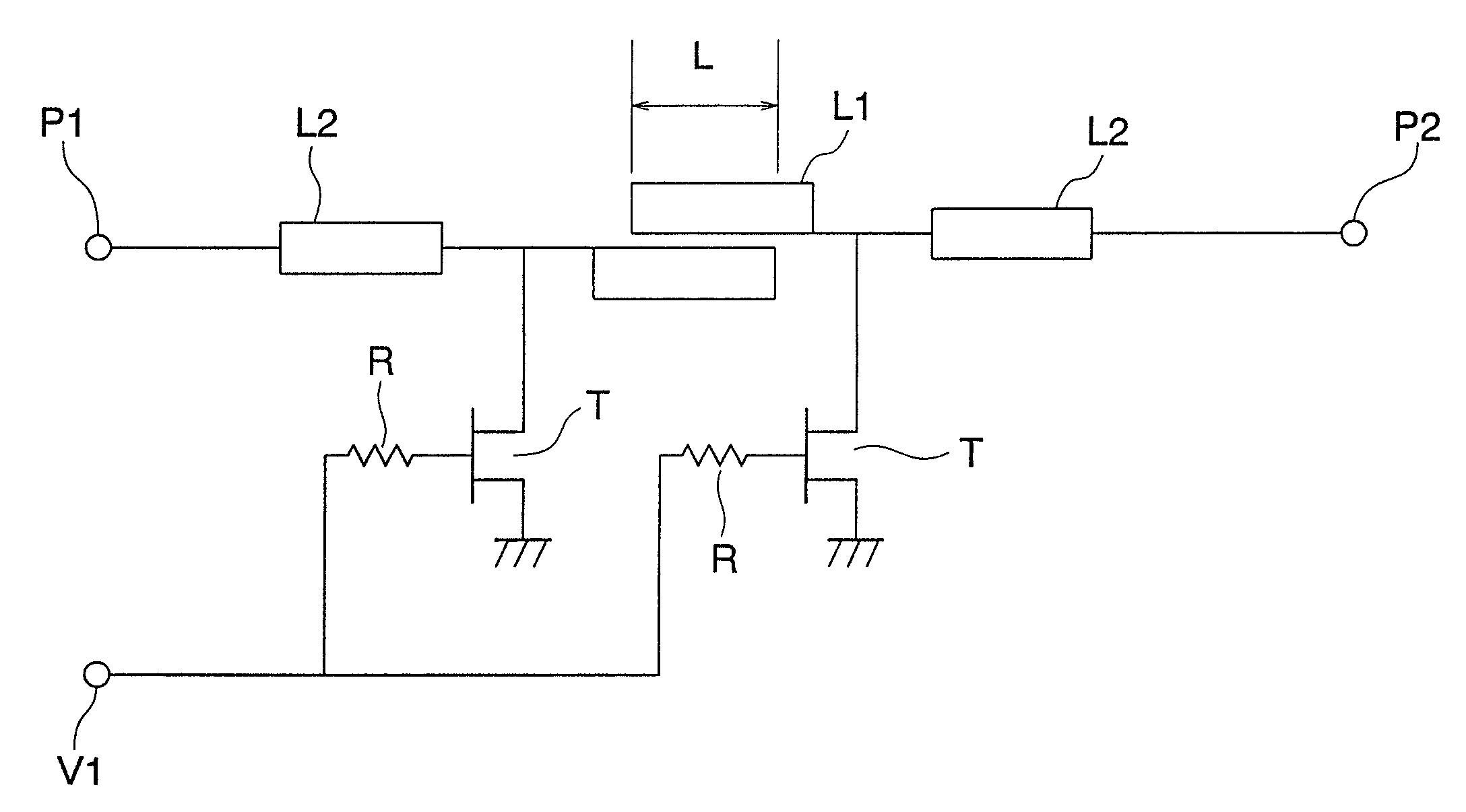
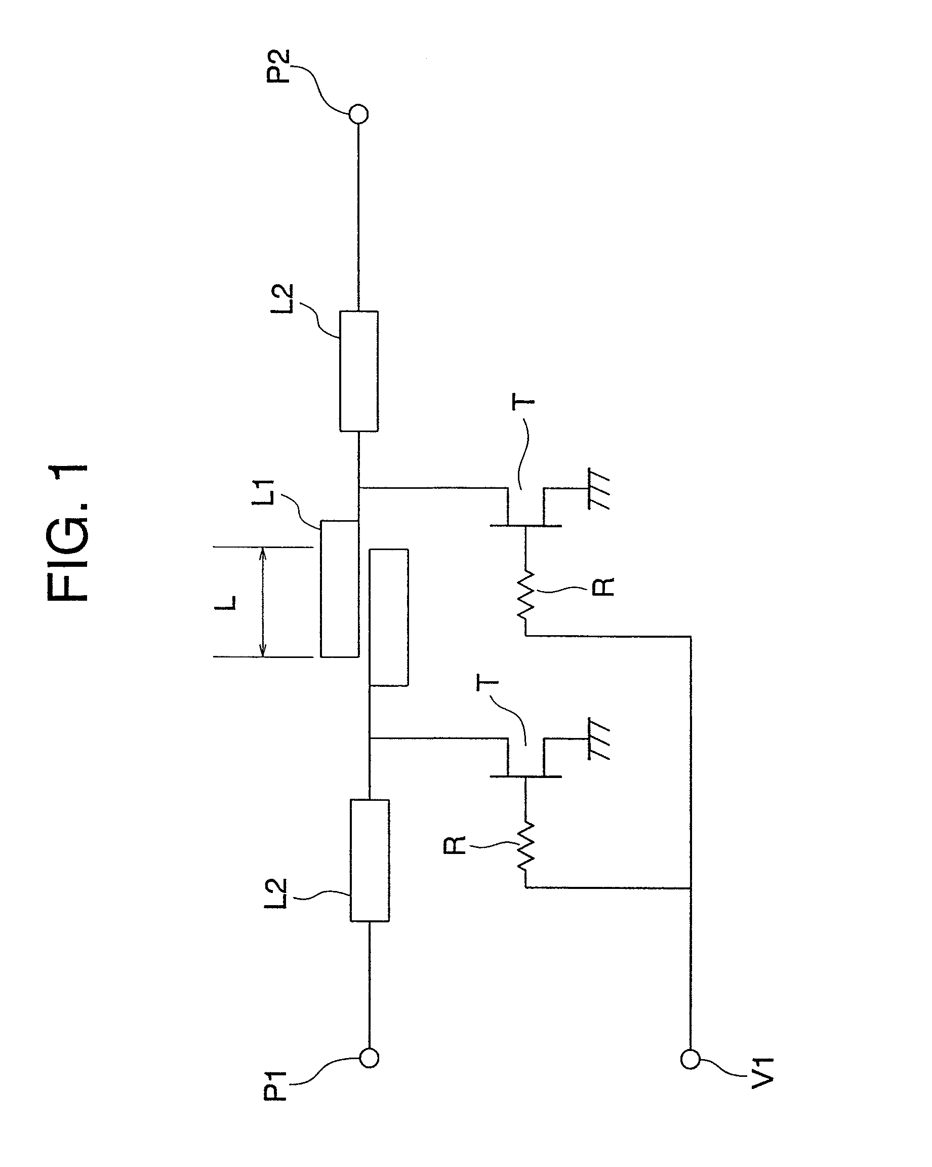
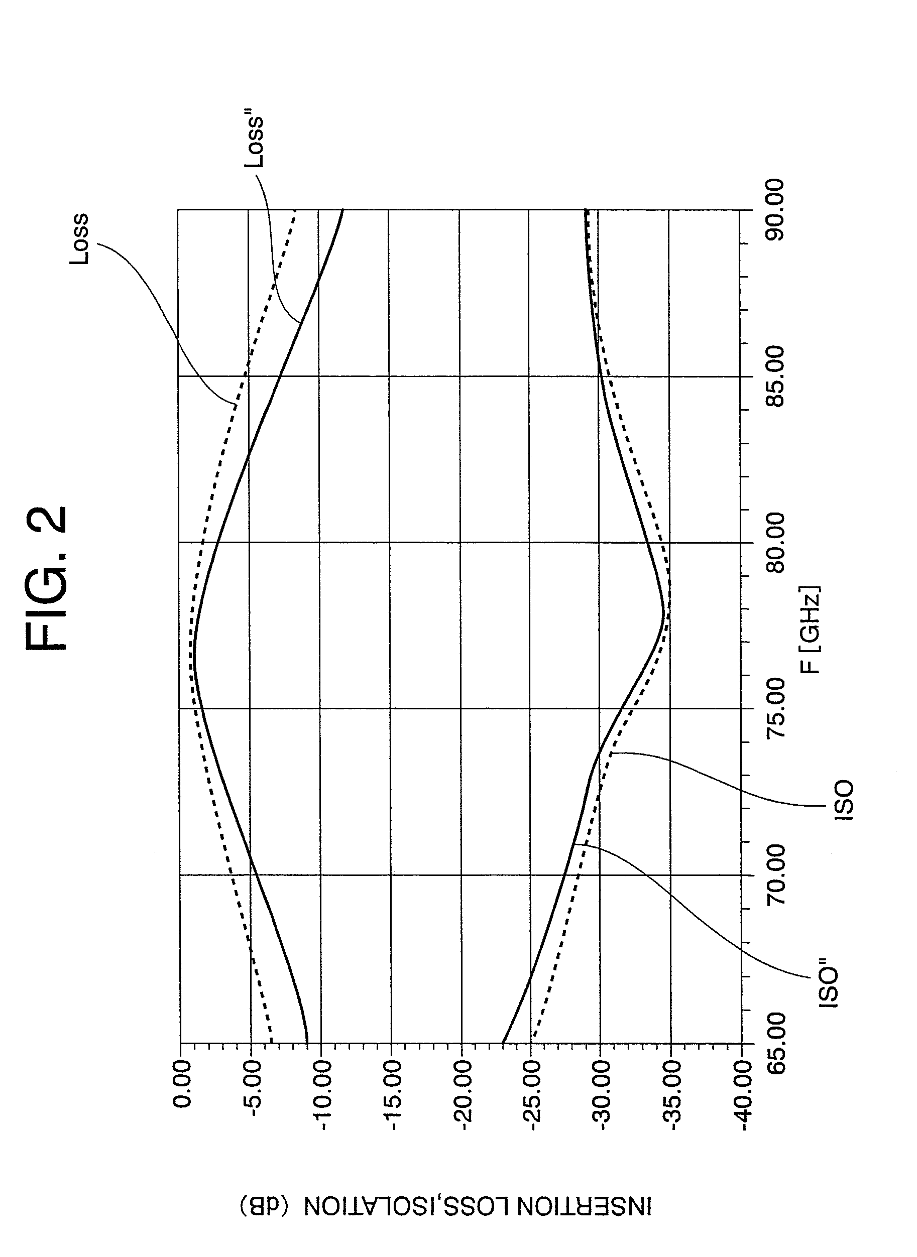
[0030]A millimeter-band SPST switching circuit according to Embodiment 1 of the present invention will be described with reference to FIGS. 1 and 2. FIG. 1 is an equivalent circuit diagram showing a structure of the millimeter-band SPST switching circuit according to Embodiment 1 of the present invention. Hereinafter, in each of the drawings, the same reference symbols indicate the same or corresponding portions.

[0031]The millimeter-band SPST switching circuit according to Embodiment 1 of the present invention as shown in FIG. 1 includes a transmission line (first transmission line) L2 connected with a signal input and output terminal P1, a transmission line (second transmission line) L2 connected with a signal input and output terminal P2, a coupling line L1 which is connected between the two transmission lines L2 and has a length L, a field effect transistor (FET) (first switching element) T whose gate is connected with a control voltage application terminal V1 through a bias resi...

embodiment 2

[0039]A millimeter-band SPDT switching circuit according to Embodiment 2 of the present invention will be described with reference to FIG. 3. FIG. 3 is an equivalent circuit diagram showing a structure of the millimeter-band SPDT switching circuit according to Embodiment 2 of the present invention.

[0040]The millimeter-band SPDT switching circuit according to Embodiment 2 of the present invention as shown in FIG. 3 includes a transmission line (first transmission line) L5 connected between a signal input and output terminal (first input and output terminal) P0 and a branch point PP, the coupling line (first coupling line) L1 which has the length L and is located on the left side, the transmission line (second transmission line) L2 connected with the signal input and output terminal (second input and output terminal) P1, a transmission line (third transmission line) L3 which is connected with the branch point PP and located on the left side, the field effect transistor (FET) (first sw...

embodiment 3

[0047]A millimeter-band switching circuit according to Embodiment 3 of the present invention will be described with reference to FIG. 4. FIG. 4 is an equivalent circuit diagram showing a structure of the millimeter-band switching circuit according to Embodiment 3 of the present invention.

[0048]The millimeter-band switching circuit according to Embodiment 3 of the present invention as shown in FIG. 4 includes the transmission line L5 connected between the signal input and output terminal P0 and the branch point PP, the first coupling line L1 having the length L, the transmission line L2 connected with the signal input and output terminal P1, the first transmission line L3 connected with the branch point PP, the field effect transistor (FET) T whose gate is connected with the control voltage application terminal V1 through the bias resistor R, whose drain is connected with the transmission line L2 and the coupling line L1, and whose source is grounded, and the field effect transistor ...


PUM


Abstract

A millimeter-band switching circuit easily corrects a varied off capacitance of a switching element without shifting position of the switching element. The millimeter-band switching circuit includes: a coupling line having a line length that can be changed; a first input and output terminal; a second input and output terminal; a first transmission line connected between the first input and output terminal and a first end of the coupling line; a second transmission line connected between the input and output terminal and a second end of the coupling line; a first field effect transistor (FET) connected in parallel with the first transmission line; and a second FET connected in parallel with the second transmission line and turned ON / OFF simultaneously with turning ON / OFF of the first FET.

Description

BACKGROUND OF THE INVENTION[0001]1. Field of the Invention[0002]The present invention relates to a millimeter-band switching circuit which operates in a millimeter-band.[0003]2. Description of the Related Art[0004]In a general millimeter-band switching circuit, switching elements are connected in parallel with a signal line to reduce an insertion loss. In order to ensure isolation, two or more switching elements are connected with one another through a transmission line.[0005]A known millimeter-band single-pole single-throw (SPST) switching circuit will be described with reference to FIGS. 7 and 8. FIG. 7 is an equivalent circuit diagram showing a structure of the known millimeter-band SPST switching circuit (see, for example, JP 09-093001 A). FIG. 8 shows an insertion loss and an isolation characteristic of the known millimeter-band SPST switching circuit. The characteristics shown in FIG. 8 are obtained by simulation.[0006]The known millimeter-band SPST switching circuit shown in ...

Claims


Application Information

Patent Timeline
Patent Type & Authority Patents(United States)
IPC IPC(8): H01P1/10H01P5/04
CPCH01P1/15
Inventor TSUKAHARA, YOSHIHIRO
Owner MITSUBISHI ELECTRIC CORP
Why Eureka
Try Eureka