Semiconductor device

a semiconductor device and semiconductor technology, applied in the field of semiconductor devices, can solve the problems of difficult demodulation of carrier waves whose modulation factor is small, interference in and difficulty in obtaining power from a power supply, so as to prevent the device from being disabled or malfunctioning, the effect of stably transmitting and not hindering the operation of the semiconductor devi

Active Publication Date: 2010-03-25
SEMICON ENERGY LAB CO LTD
View PDF11 Cites 12 Cited by
  • Summary
  • Abstract
  • Description
  • Claims
  • Application Information

AI Technical Summary

Benefits of technology

[0010]In general, a reception side device includes an analog circuit having a demodulation circuit, a power supply circuit, a modulation circuit, and the like, and a digital circuit connected to the analog circuit. As an output of the demodulation circuit, a demodulation signal is output from the analog circuit and input into the digital circuit. When a carrier wave whose modulation factor is 100% is used for wireless communication, a state in which an amplitude is 0 (a state in which an amplitude peak and a reference line accord with each other) is included. Therefore, in particular, in a semiconductor device which operates by generating power from a power supply through a received electromagnetic wave, it is difficult to obtain power from a power supply when an amplitude of a carrier wave whose modulation factor is 100%, which is used for wireless communication, is 0. Accordingly, the operation of the semiconductor device is interfered. In such a semiconductor device, a certain amplitude is secured so as to supply power with the use of a carrier wave whose modulation factor is small (for example, a carrier wave whose modulation factor is 10%); thus, the semiconductor device can be operated.
[0021]In addition, another object of one embodiment of the present invention is to provide a card (or chip) which can stably transmit and receive data to and from a reader / writer even in the case where there is a plurality of cards (or chips) on which semiconductor devices that can transmit and receive data to and from the reader / writer are mounted.
[0027]Further, when an antenna circuit transmits data, a signal demodulated by the first demodulation signal generation circuit is selected by the logic circuit, and when the antenna circuit receives data, a signal demodulated by the second demodulation signal generation circuit is selected by the logic circuit. Therefore, even when the semiconductor device receives a transmission signal to the reader / writer, the transmission signal is not demodulated again, so that the operation of the semiconductor device is not hindered by the transmission signal. Thus, in a card (or chip) on which the semiconductor device is mounted, the card can be prevented from being disabled or malfunctioning due to the card itself, and data can be stably transmitted and received to and from the reader / writer.
[0028]Further, when the antenna circuit transmits data, the signal demodulated by the first demodulation signal generation circuit is selected by the logic circuit, and when the antenna circuit receives data, the signal demodulated by the second demodulation signal generation circuit is selected by the logic circuit. Therefore, even in the case where there is a plurality of cards (or chips) other than a card on which the semiconductor device is mounted (hereinafter referred to as one card) in a range where the one card is operated by a magnetic field that is generated by the reader / writer, transmission signals from the other cards are not demodulated even when the transmission signals are received by the one card. Accordingly, the one card can be prevented from being disabled or malfunctioning due to the other cards, whereby data can be stably transmitted and received to and from the reader / writer.

Problems solved by technology

Therefore, in particular, in a semiconductor device which operates by generating power from a power supply through a received electromagnetic wave, it is difficult to obtain power from a power supply when an amplitude of a carrier wave whose modulation factor is 100%, which is used for wireless communication, is 0.
Accordingly, the operation of the semiconductor device is interfered.
Although the circuit illustrated in FIG. 5 can demodulate a carrier wave whose modulation factor is large (for example, a carrier wave whose modulation factor is 100%), it is difficult to demodulate a carrier wave whose modulation factor is small (for example, a carrier wave whose modulation factor is 10%).

Method used


Image

  • Semiconductor device
  • Semiconductor device
  • Semiconductor device

Examples


embodiment 1

[0045]In this embodiment, an example of a structure of a semiconductor device will be described with reference to FIG. 1, FIG. 2, FIG. 3, FIG. 4, FIG. 5, FIG. 6, FIGS. 7A to 7E, FIGS. 8A to 8D, FIG. 9, FIG. 10, FIGS. 11A and 11B, FIG. 12, and FIGS. 13A to 13E.

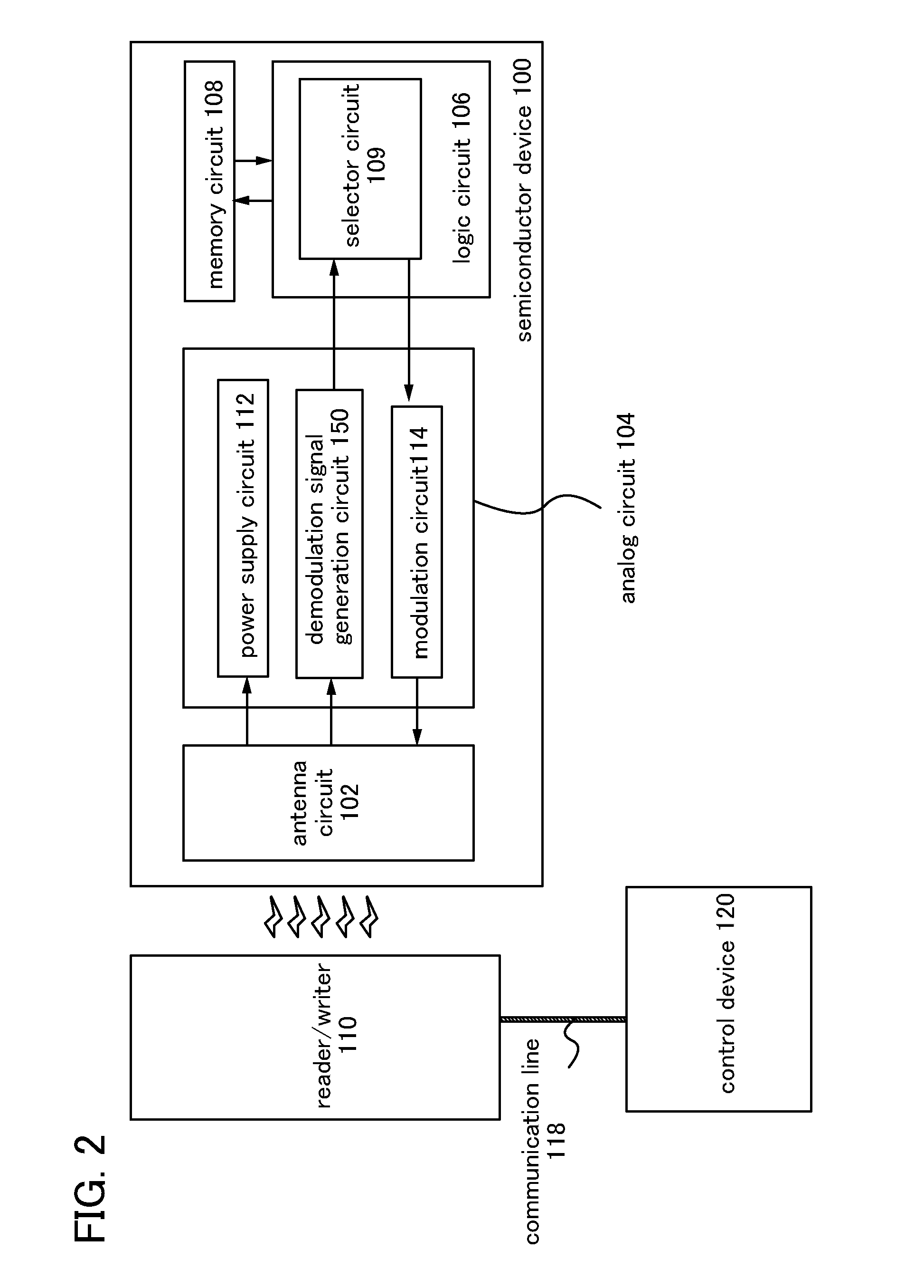
[0046]A semiconductor device of this embodiment is illustrated in FIG. 2. In FIG. 2, a semiconductor device 100 transmits and receives data wirelessly to and from a reader / writer 110 by an electromagnetic wave. Further, the semiconductor device 100 is wirelessly supplied with power from the reader / writer 110.

[0047]The reader / writer 110 is preferably connected to a control device 120 through a communication line 118. The control device 120 controls communication between the reader / writer 110 and the semiconductor device 100.

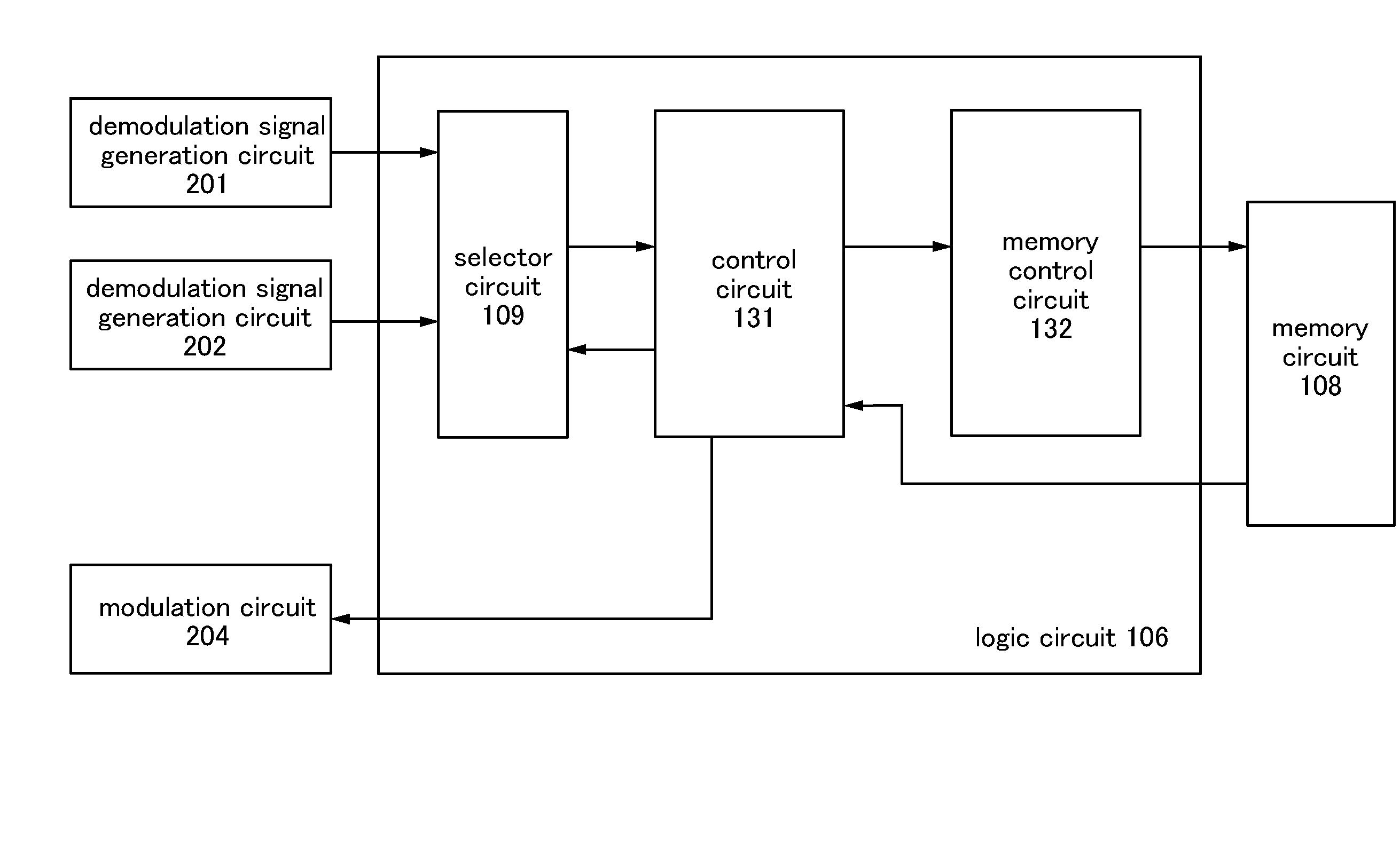
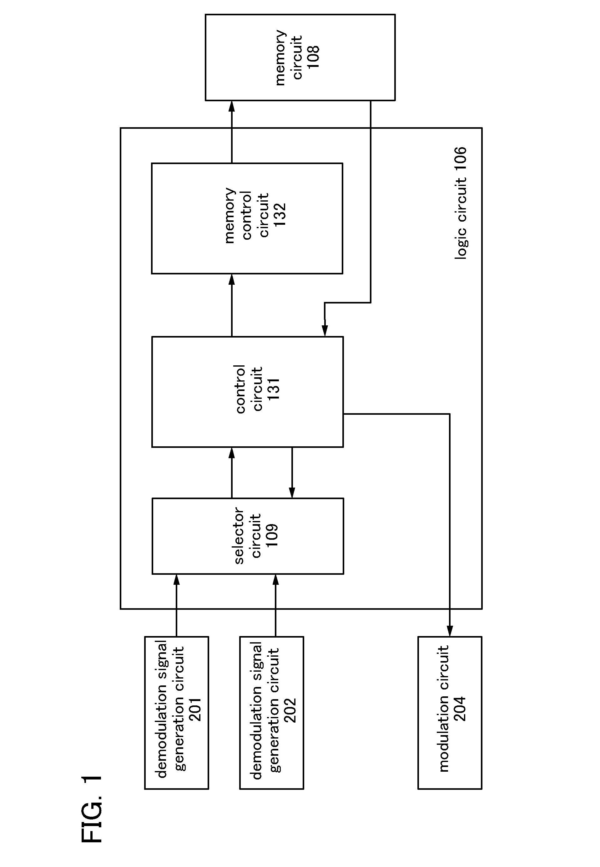
[0048]The semiconductor device 100 includes an antenna circuit 102, an analog circuit 104, a logic circuit 106, and a memory circuit 108. The analog circuit 104 has a demodulation signal generation circuit 15...

embodiment 2

[0127]This embodiment will describe an example of a structure of a semiconductor device in a mode which is different from Embodiment 1. Specifically, this embodiment will employ a structure in which the semiconductor device described in Embodiment 1 is provided with a battery.

[0128]A semiconductor device of this embodiment is illustrated in FIG. 15. In FIG. 15, a semiconductor device 1800 transmits and receives data wirelessly to and from a reader / writer 1811 by an electromagnetic wave. Further, the semiconductor device 1800 is wirelessly supplied with power from the reader / writer 1811.

[0129]The reader / writer 1811 is preferably connected to a control device 1813 through a communication line 1812. The control device 1813 controls communication between the reader / writer 1811 and the semiconductor device 1800.

[0130]The semiconductor device 1800 includes an antenna circuit 1802, an analog circuit 1824, a logic circuit 1809, a memory circuit 1810, and a battery 1804. The analog circuit 1...

embodiment 3

[0160]A semiconductor device which is manufactured by applying any of the foregoing embodiments can be used for various objects and systems utilizing a function of transmitting or receiving electromagnetic waves. Examples in which a semiconductor device 2000 using any of the foregoing embodiments is mounted are illustrated in FIGS. 14A to 14F.

[0161]As items having the semiconductor device of any of the foregoing embodiments, the following items are given: keys (see FIG. 14A), paper money, coins, securities, bearer bonds, certificates (such as a driver's license or a resident's card, see FIG. 14B), books, containers (such as a Petri dish, see FIG. 14C), packaging containers (such as wrapping paper or bottles, see FIGS. 14E and 14F), recording media (such as a disk or video tape), vehicles (such as a bicycle), personal accessories (such as bags or eyeglasses, see FIG. 14D), food, clothing, livingware, electronic appliances (such as a liquid crystal display device, an EL display device...


PUM


Abstract

To provide a semiconductor device which can transmit / receive data to / from a reader / writer without interruption of operation by the reader / writer or the like. A semiconductor device capable of wireless communication includes an antenna circuit, a first demodulation signal generation circuit which demodulates a signal whose modulation factor is from 95% to 100%, both inclusive, a second demodulation signal generation circuit which demodulates a signal whose modulation factor is from 95% and 100%, both inclusive and from 10% and 30%, both inclusive and a logic circuit which selects one of a demodulation signal from the first circuit and a demodulation signal from the second circuit. When the antenna circuit receives an electromagnetic wave, the logic circuit selects the demodulation signal from the second circuit, and when the antenna circuit transmits an electromagnetic wave, the logic circuit selects the demodulation signal from the first circuit.

Description

TECHNICAL FIELD[0001]The present invention relates to a semiconductor device which can transmit and receive information without contact by utilizing wireless communication, and relates to a card on which the semiconductor device is mounted.BACKGROUND ART[0002]In recent years, individual recognition technology in which individual identification information is given to an individual object to clarify information such as a history of the object has attracted attention. In particular, the development of semiconductor devices which can transmit and receive data without contact by utilizing wireless communication through a radio wave has been advanced. Such semiconductor devices are referred to as an IC tag, an RFID tag, and the like, which have begun to be used for management of articles in markets, or the like.[0003]In general, many of objects which are referred to as an RFID tag and the like that have been put into practical use include an element formation layer and an antenna layer e...

Claims


Application Information

Patent Timeline
Patent Type & Authority Applications(United States)
IPC IPC(8): H04Q5/22
CPCH04Q2213/13095G06K19/0723H04B5/0037H04B5/0031H04L27/04H04L27/06
Inventor KOBAYASHI, HIDETOMO
Owner SEMICON ENERGY LAB CO LTD
Why Eureka
Try Eureka