Wafer defect detection system and method

a defect detection and defect technology, applied in the field of wafer defect detection systems, can solve problems such as mask problems that are often associated with repeaters

Active Publication Date: 2010-03-25
APPL MATERIALS ISRAEL LTD
View PDF0 Cites 13 Cited by
  • Summary
  • Abstract
  • Description
  • Claims
  • Application Information

AI Technical Summary

Benefits of technology

[0020]Still further in accordance with at least one embodiment of the present invention, the method also comprises pruning the repeater map to eliminate die-level systematic defects.
[0028]Further in accordance with at least one embodiment of the present invention, the method also comprises initiating, upon generating a first set of defects per slice, a request for images corresponding to defects included in the first set of defects per slice; and / or upon generating a second set of defects per slice, initiating a request for images corresponding to defects included in the second set of defects per slice, thereby enabling allocation of images associated with defects included in the defect map.

Problems solved by technology

Field repeaters are often associated with mask problems, such as for example haze defects, as opposed to die-level systematic defects which are often associated with a marginal process.

Method used


Image

  • Wafer defect detection system and method
  • Wafer defect detection system and method
  • Wafer defect detection system and method

Examples


Embodiment Construction

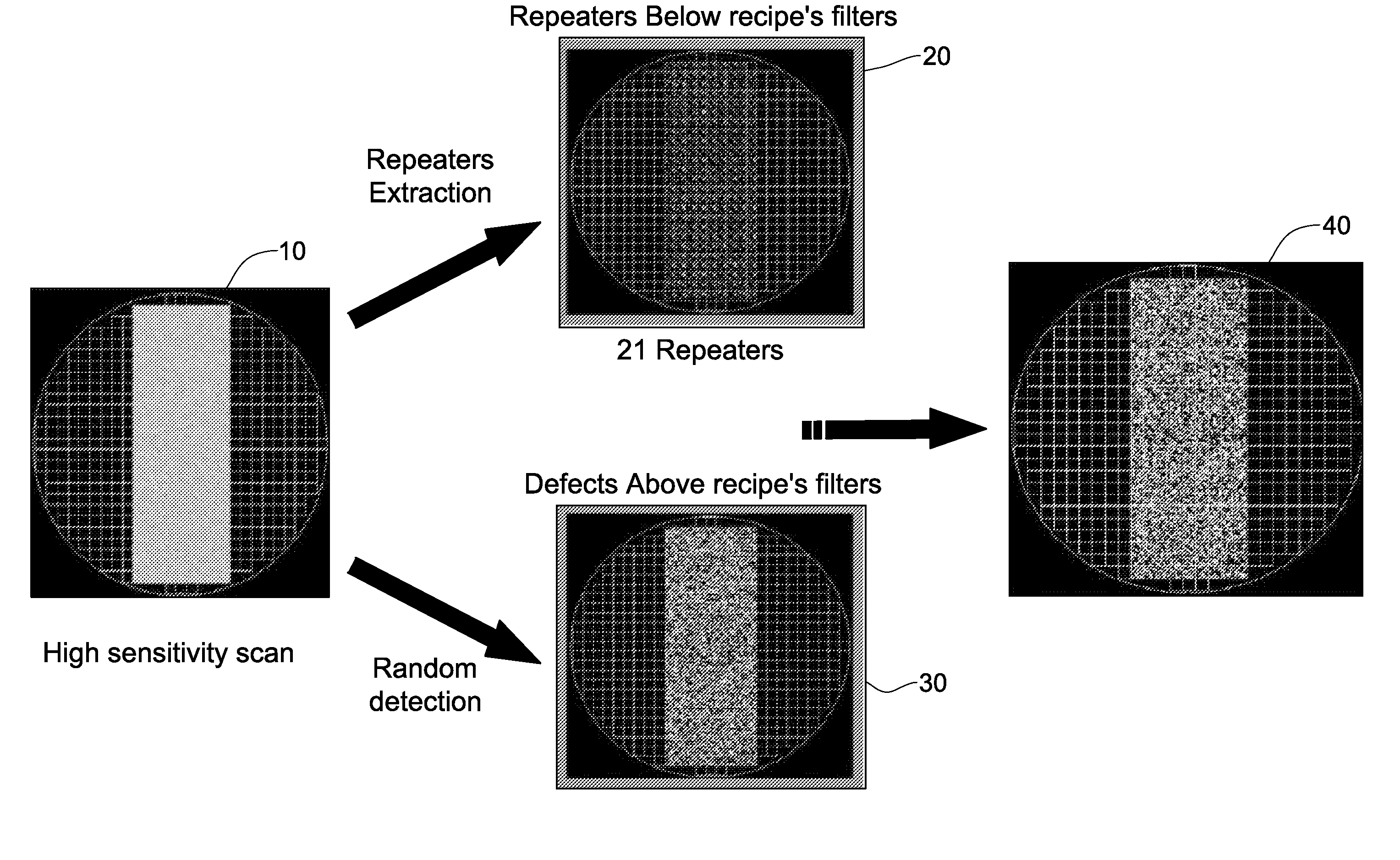
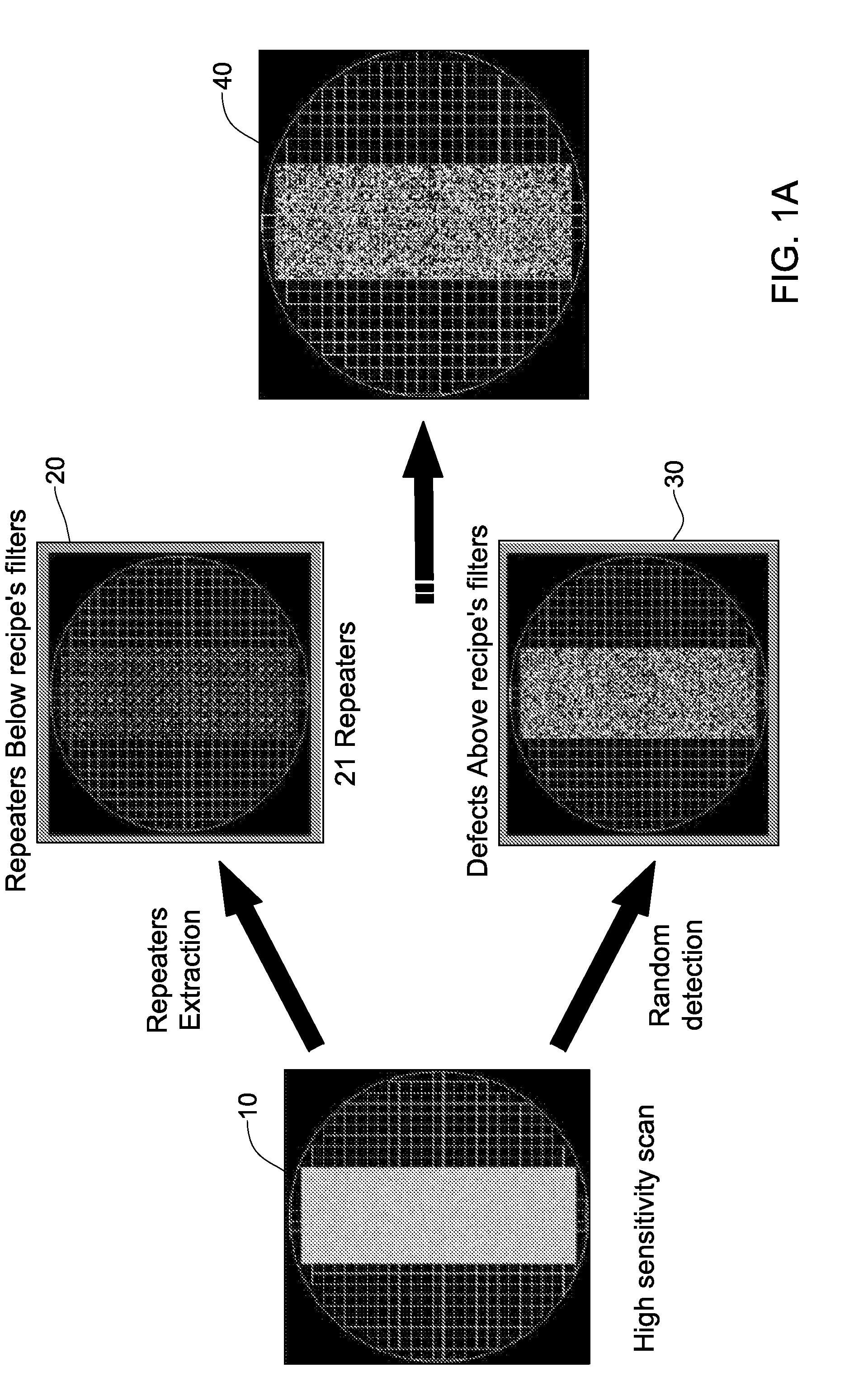
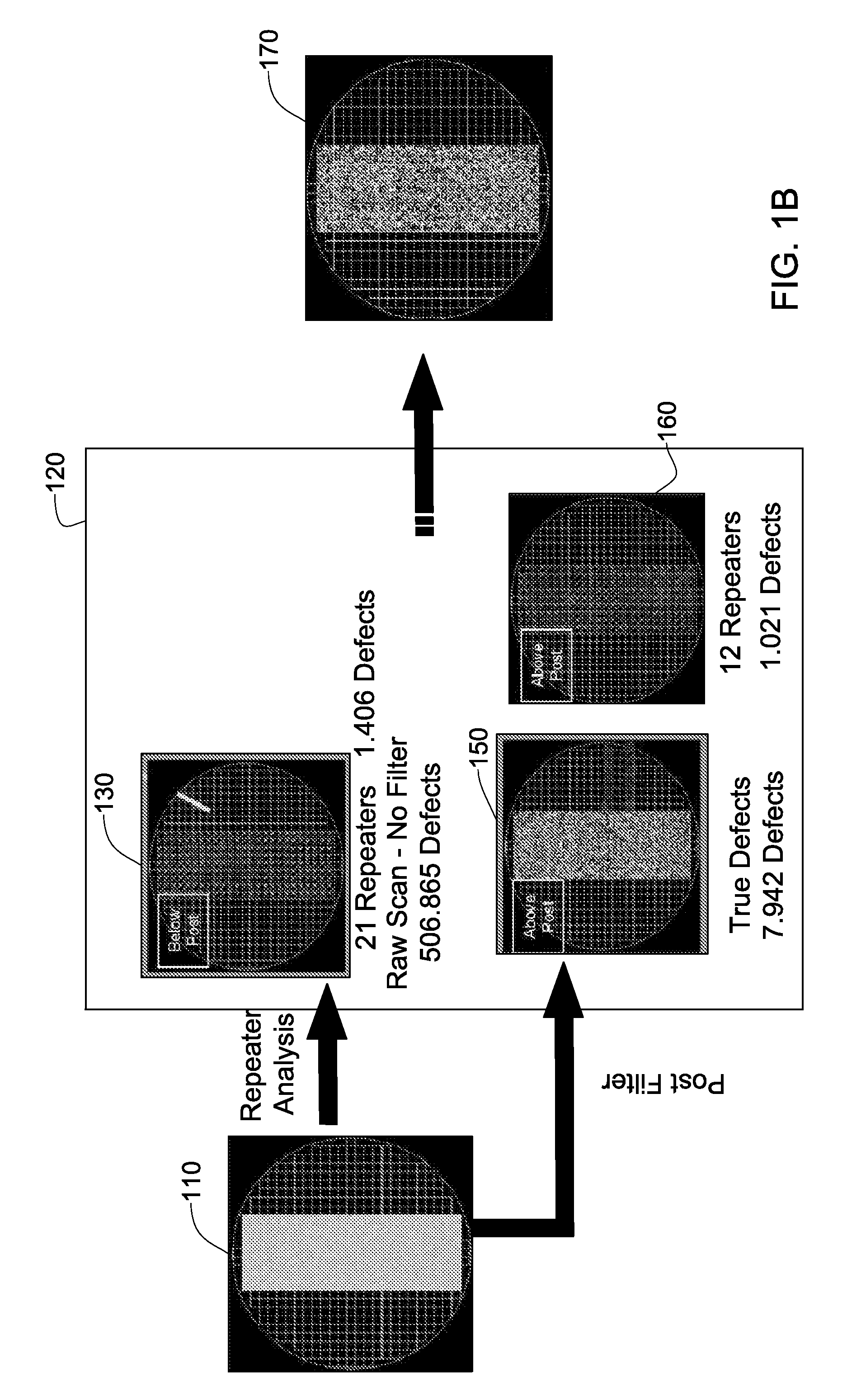
[0058]The following acronyms are used herein:[0059]A. IOD—image on demand[0060]B. OTF—on the fly images[0061]C. C2C—Cell 2 Cell detection, for which a purifier as described herein may be employed, even in fields including 2 dies in the direction of D2D detection.[0062]D. V / G, V-G: Volume grade filter, or a functionality which filters out defects based on the volume and / or grade thereof.[0063]E. BB—bounding box[0064]F. AR—aspect ratio[0065]G. IP—image processor[0066]H. CR—capture rate[0067]I. RBP—repeater below post[0068]J. NF—nuisance filter[0069]K. ADI (gate ADI layer)—“after-develop inspect”, namely a layer in semiconductor processing)[0070]L. STI—short trench isolation[0071]M. TPT—throughput[0072]N. SR—search radius for repeater analysis. Two defects that are within this distance in field coordinates of each other may be either deemed to belong to the same repeater family or to comprise a pair of non-repeaters.[0073]O. IP—image processor.

[0074]The following terms may be construed...


PUM

PropertyMeasurementUnit
defectaaaaaaaaaa
defectsaaaaaaaaaa
thresholdaaaaaaaaaa

Abstract

Random defects and repeaters accommodated on a wafer are detected using slice information obtained by scanning a plurality of wafer slices; analyzing defect information using a first set of filters selected to detect random defects, thereby generating a first set of defects per slice, analyzing the defect information using a second set of filters selected to detect repeaters, thereby providing a second set of defects per slice; analyzing a plurality of the second sets of defects per slice using a third set of filters selected to detect repeater families, thereby providing a set of repeaters per wafer; and optionally combining the set of repeaters per wafer with a plurality of the first sets of defects per slice, thereby generating one or more defect maps indicative of random defects and / or repeaters.

Description

REFERENCE TO CO-PENDING APPLICATIONS[0001]Priority is claimed from U.S. provisional application No. 61 / 099,812, entitled “High Sensitivity Repeater Detection in Wafer Inspection”, filed 24 Sep. 2008, incorporated herein by reference.FIELD OF THE INVENTION[0002]The present invention relates generally to wafer defect detection systems.BACKGROUND OF THE INVENTION[0003]Many wafer defect detection systems are known in the art.[0004]The disclosures of all publications and patent documents mentioned in the specification, and of the publications and patent documents cited therein directly or indirectly, are hereby incorporated by reference.SUMMARY OF THE INVENTION[0005]Repeater Defects or “field repeaters” are systematic defects which appear at a specific location in a field. Field repeaters are often associated with mask problems, such as for example haze defects, as opposed to die-level systematic defects which are often associated with a marginal process. Conventionally, repeater analysi...

Claims


Application Information

Patent Timeline
Patent Type & Authority Applications(United States)
IPC IPC(8): G06F19/00G01N21/00
CPCG01N21/9501
Inventor AUERBACH, DITZA
Owner APPL MATERIALS ISRAEL LTD
Why Eureka
Try Eureka