
Integrated multicomponent device in a semiconducting die

Active Publication Date: 2010-08-05
COMMISSARIAT A LENERGIE ATOMIQUE ET AUX ENERGIES ALTERNATIVES
View PDF25 Cites 36 Cited by
  • Summary
  • Abstract
  • Description
  • Claims
  • Application Information

AI Technical Summary

Benefits of technology

[0037]The material of the wafer and the coating material may have properties with which problems encountered with kno

Problems solved by technology

By using a double face thermosensitive adhesive layer, adhesion with the wafer, but also with the support, may be broken.

Method used


Image

  • Integrated multicomponent device in a semiconducting die
  • Integrated multicomponent device in a semiconducting die
  • Integrated multicomponent device in a semiconducting die

Examples


Embodiment Construction

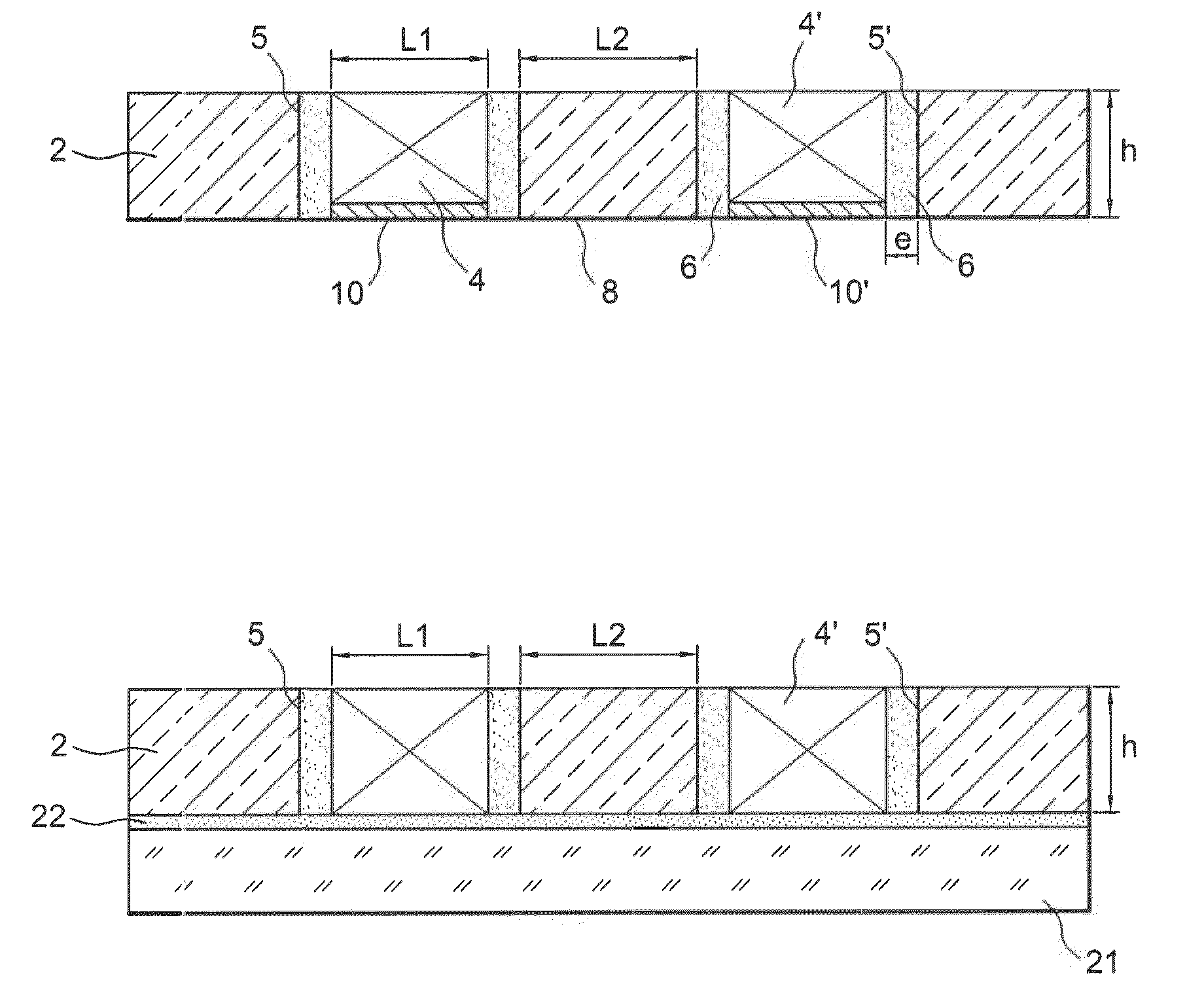
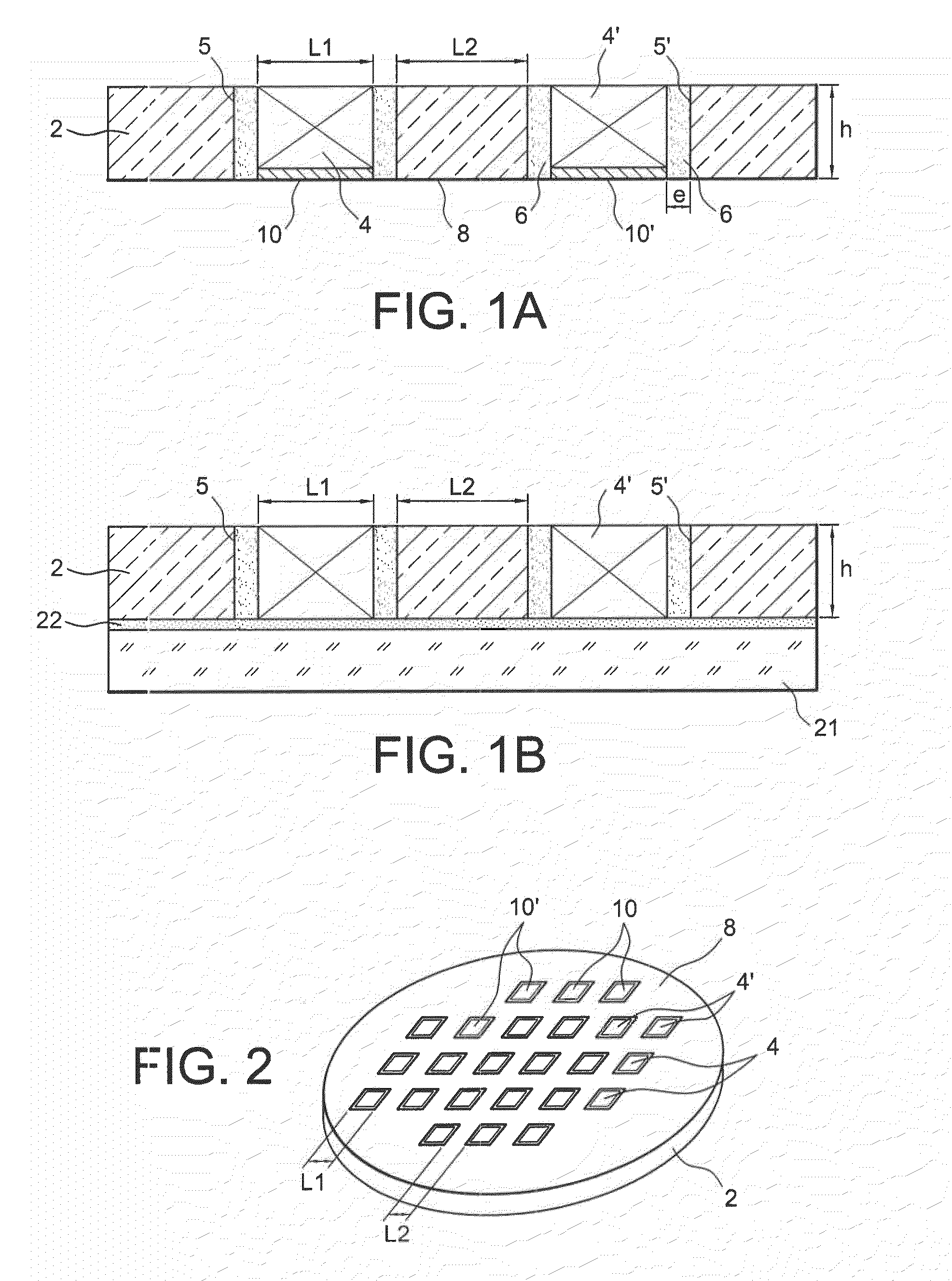
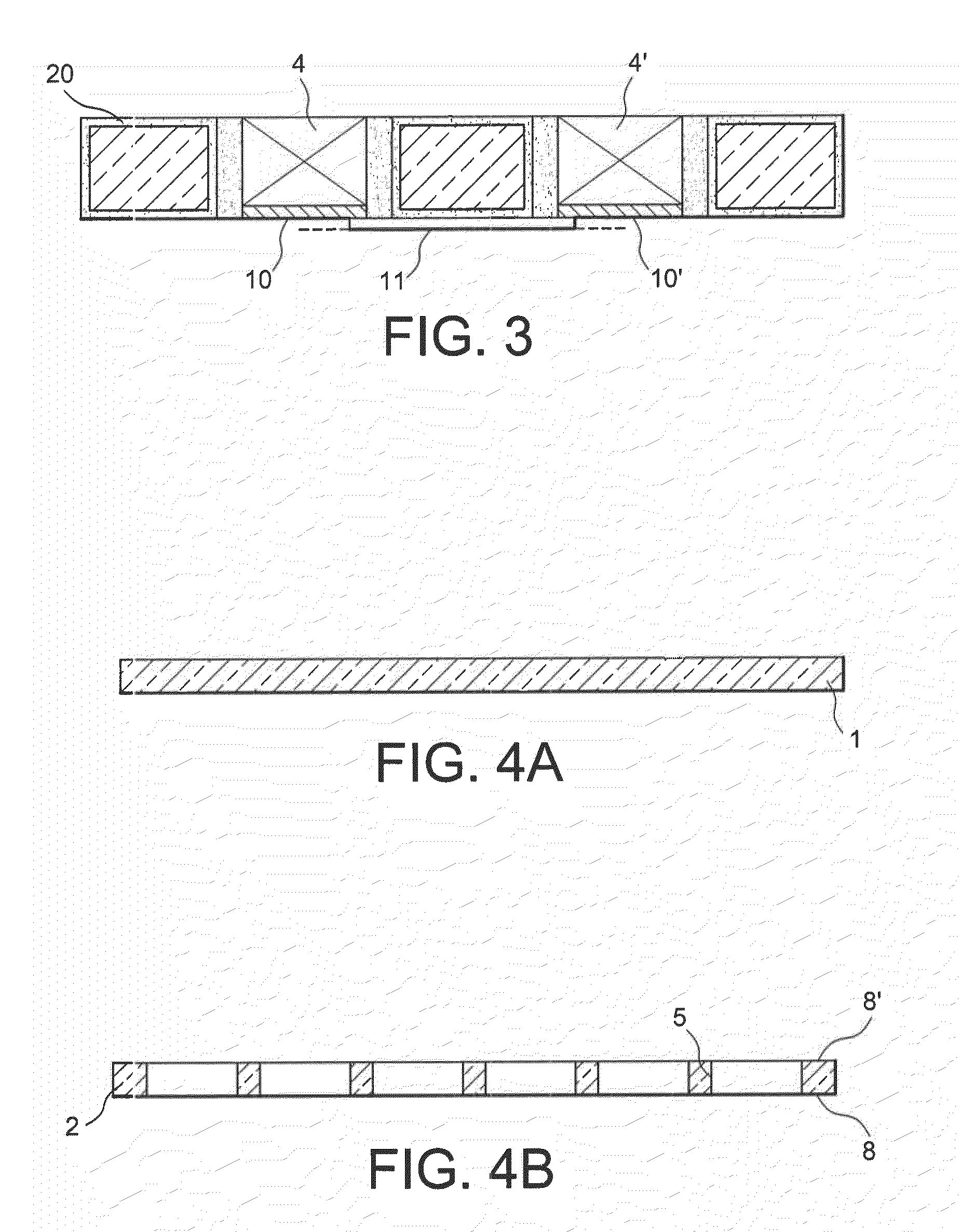
[0056]Two examples of devices which may be obtained by the invention are illustrated in a sectional view in FIGS. 1A and 1B.

[0057]Each of these two devices includes a die 2, for example in a semiconducting material, with a thickness h. One or more electronic components 4, 4′ which may either be all identical or different from each other (they may notably have thicknesses different from each other), are contained in cavities 5, 5′ of this die. The active faces of these components are designated by references 10, 10′: these are faces on which are made elementary components defining the functionalities of each component. These active faces 10, 10′ of the components are flush with the plane of the face 8, a so-called front face, of the receiving die 2. One or more of the components 4 may be semiconducting components, in particular from the field of micro-electronics, such as integrated circuits and / or MEMS sensors, and / or optical components (MOEMS) and / or bio-components and / or switches....


PUM

PropertyMeasurementUnit
Fractionaaaaaaaaaa
Temperature coefficient of resistanceaaaaaaaaaa

Abstract

An electronic device with integrated discrete components, including a wafer including cavities that can receive the components, an active face of the components being in a same plane as a face of the receiving wafer, and a material for laterally coating the components in the cavities.The invention relates to an electronic device with integrated discrete components (4), including:a wafer (2), a so-called receiving wafer, said wafer having cavities (5, 5′) containing said components, the active face (10) of which is in a same plane as a face (8) of the receiving wafer,a material (6) for laterally coating the components in the cavities.

Description

TECHNICAL FIELD AND PRIOR ART[0001]The field of the invention relates to the assembling of microsystems on a scale of a wafer in a semiconducting material, for example in silicon.[0002]It notably relates to applications for which technologies are sought, commonly called “Above IC”, for high density integration of passive components, of detectors or optoelectronic components or of MEMs directly on the circuits.[0003]Presently, heterogeneous integration methods can only be accomplished on entire silicon wafers. The “Above IC” methods are therefore limited to the fields where the microsystem integrator may have wafers available, which involves significant costs (from a few hundred thousand euros to several million euros with switching to 300 mm wafers) in terms of sets of masks and of manufacturing the wafers in a foundry. In this context, it is understandable that these costs are an obstacle to the emergence of novel technologies and that the actors are very restricted.[0004]Further, ...

Claims


Application Information

Patent Timeline
IPC IPC(8): H05K7/06H05K3/30
CPCB81C1/0023Y10T29/49146H01L21/6835H01L23/13H01L23/147H01L23/5389H01L24/13H01L24/96H01L25/0655H01L25/50H01L2924/01003H01L2924/01013H01L2924/01027H01L2924/01049H01L2924/01057H01L2924/01058H01L2924/01061H01L2924/01075H01L2924/14H01L2924/19041H01L2924/19042H01L2924/19043H01L2924/30107H01L2924/01005H01L2924/01006H01L2924/01033H01L2924/01087H01L2924/1461H01L21/568H01L2924/00H01L2924/00014H01L2924/00011H01L2924/3511H01L2224/0401
Inventor SOURIAU, JEAN-CHARLESBALERAS, FRANCOIS
Owner COMMISSARIAT A LENERGIE ATOMIQUE ET AUX ENERGIES ALTERNATIVES
Learn More