Data processing interface device

Active Publication Date: 2010-08-19
ADVANCED MICRO DEVICES INC
View PDF2 Cites 8 Cited by
  • Summary
  • Abstract
  • Description
  • Claims
  • Application Information

AI Technical Summary

Problems solved by technology

Packaging technology limits how physically small these electrical connections can be and therefore limits the number of individual pins that can be incorporated on a particular IC die.
Therefore, the number of pins that can be physically disposed at an IC die can limit the number of circuit components that can be included at an individual IC die.
Providing a signal interface to multiple IC die incorporated at an MCM is particularly difficult.

Method used


Image

  • Data processing interface device
  • Data processing interface device
  • Data processing interface device

Examples


Embodiment Construction

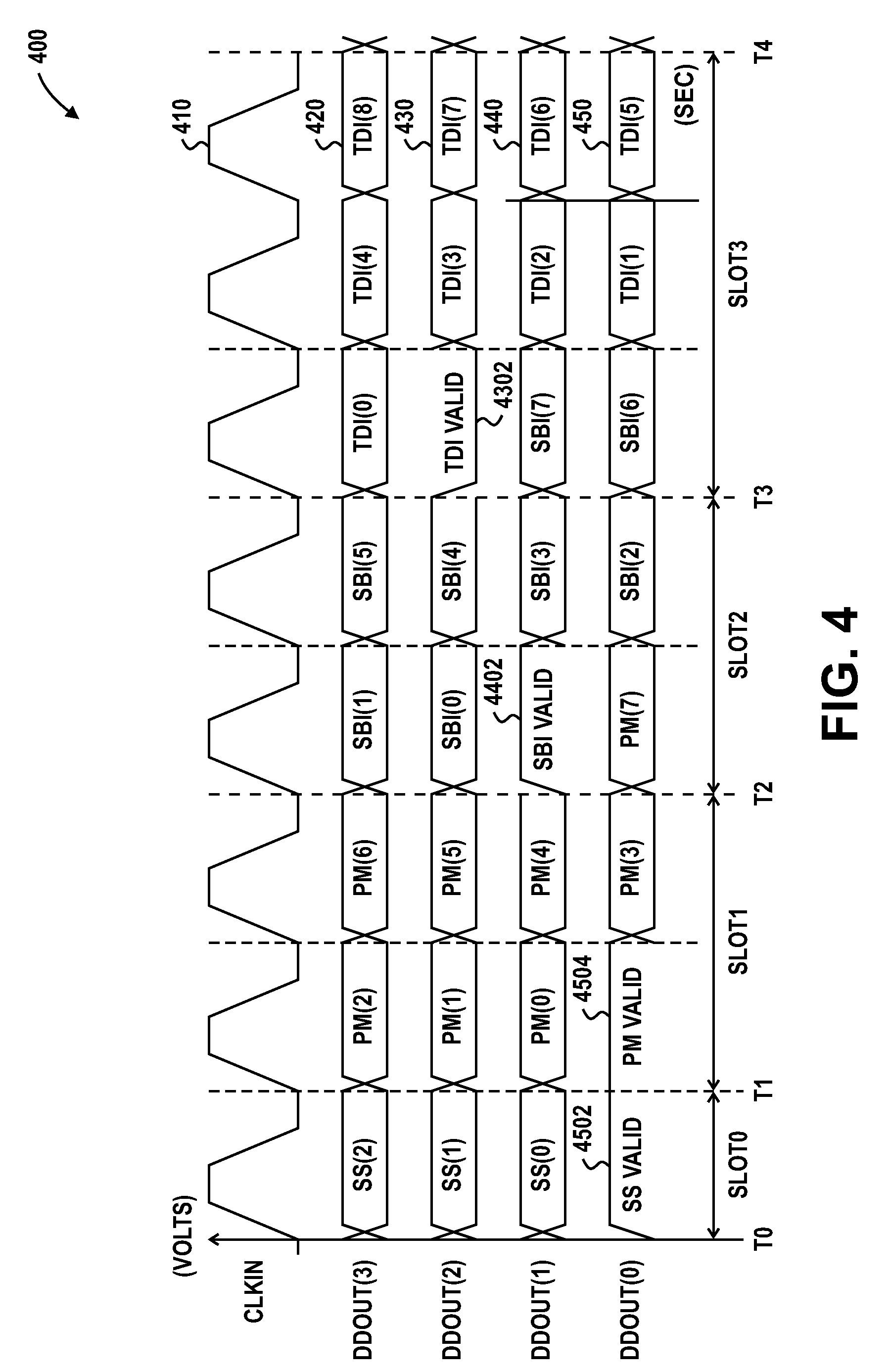
[0012]A device and method are disclosed to provide a die-to-die communication link (DDCL) to facilitate the exchange of information of different types between two or more IC die included at a data processing device using a time-divided multiplexed protocol.

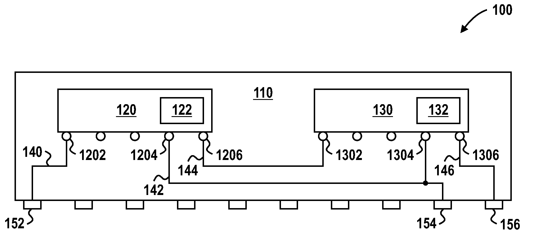
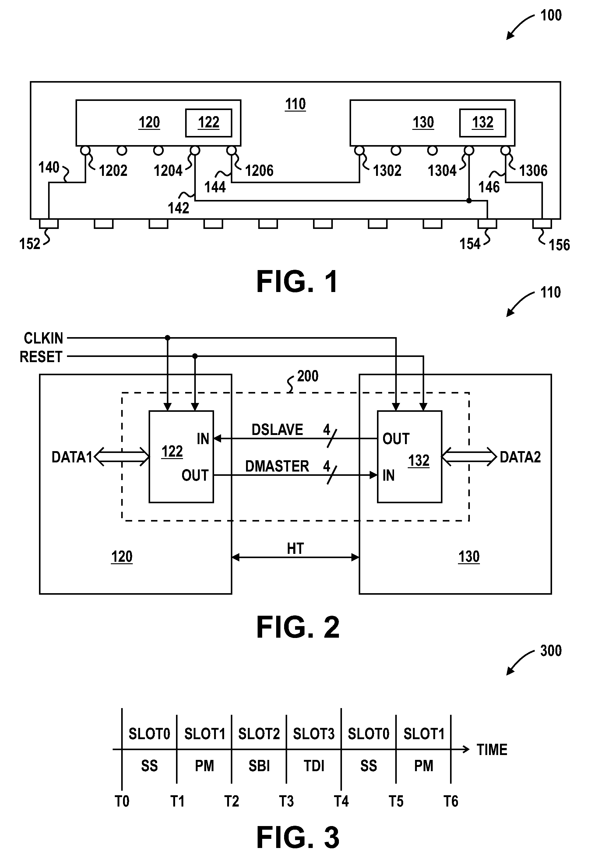
[0013]FIG. 1 illustrates a cross sectional view of a MCM 110 included at a data processing system 100 in accordance with a specific embodiment of the present disclosure. MCM 110 includes IC die 120 and IC die 130, conductors 140, 142, 144, and 146, and external interface pins 152, 154, and 156. IC die 120 and IC die 130 each includes a die-to-die interface circuit (DDIC) to support the exchange of information between IC die 120 and IC die 130. IC die 120 includes DDIC 122 and pins 1202, 1204, and 1206. IC die 130 includes a DDIC 132 and pins 1302, 1304, and 1306.

[0014]IC die 120 has a pin 1202 connected to conductor 140, a pin 1204 connected to conductor 142, and a pin 1206 connected to conductor 144. IC die 130 has a pin 1302 con...


PUM


Abstract

Information of a first type is determined at an integrated circuit die of a data processing device included an integrated circuit package. The integrated circuit package includes the first integrated circuit die and a second integrated circuit die. Information of a second type is determined at the integrated circuit die. The first and second type of information is transmitted from the integrated circuit die to another integrated circuit die using a time-divided multiplexed protocol by transmitting the first information during a first time slot of the protocol and transmitting the second information during a second time slot of the protocol.

Description

BACKGROUND[0001]1. Field of the Disclosure[0002]The present disclosure relates generally to electronic devices, and more particularly to data processing devices.[0003]2. Description of the Related Art[0004]Very large-scale integration (VLSI) is the process of creating an integrated circuit (IC) by combining a large number of components at a single IC package. The IC package can include a single IC die or can include more than one IC die. An IC package that contains more than one IC die is referred to as a multi-chip module (MCM). For example, a data processing device that includes two individual microprocessor IC die can be implemented by including the two individual microprocessor IC die at a single MCM. Each IC die is manufactured individually and each IC die is bonded to a substrate included at the MCM package. The MCM package substrate includes conductors that provide electrical connections between the pins of each IC die and between pins of the IC die and external interface pin...

Claims


Application Information

Patent Timeline
IPC IPC(8): G06F19/00G01K1/00
CPCH01L2224/16H01L25/065H01L2924/00014H01L2924/00011H01L2224/0401G06F13/38G06F13/14
Inventor MADRID, PHILIP E.ENNIS, STEPHEN C.
Owner ADVANCED MICRO DEVICES INC
Why Eureka
Try Eureka