Wiring design method for wiring board

a wiring design and wiring board technology, applied in the direction of program control, manufacturing tools, instruments, etc., can solve the problems of shortening the wiring design time, affecting the design effect, and tendency of taking a longer time to design the wiring

Inactive Publication Date: 2010-08-26
KK TOSHIBA
View PDF4 Cites 9 Cited by
  • Summary
  • Abstract
  • Description
  • Claims
  • Application Information

AI Technical Summary

Problems solved by technology

This desire may be accompanied by a tendency of taking a longer time to design the wiring.
This shortens the wiring design time than the method of a designer designing the entire wiring manually.
However, as described later, such an automatic wiring method by use of the automatic wiring design apparatus may give rise to a design error referred to as a design rule error in some cases.
In such a case, it is difficult to work out a design in such a manner as to eliminate design rule errors by using the automatic wiring design apparatus.
However, wiring, if it is of a high integration, has taken a prolonged time for manual design by the designer, thus resulting in a long time to design completely.

Method used


Image

  • Wiring design method for wiring board
  • Wiring design method for wiring board
  • Wiring design method for wiring board

Examples


first embodiment

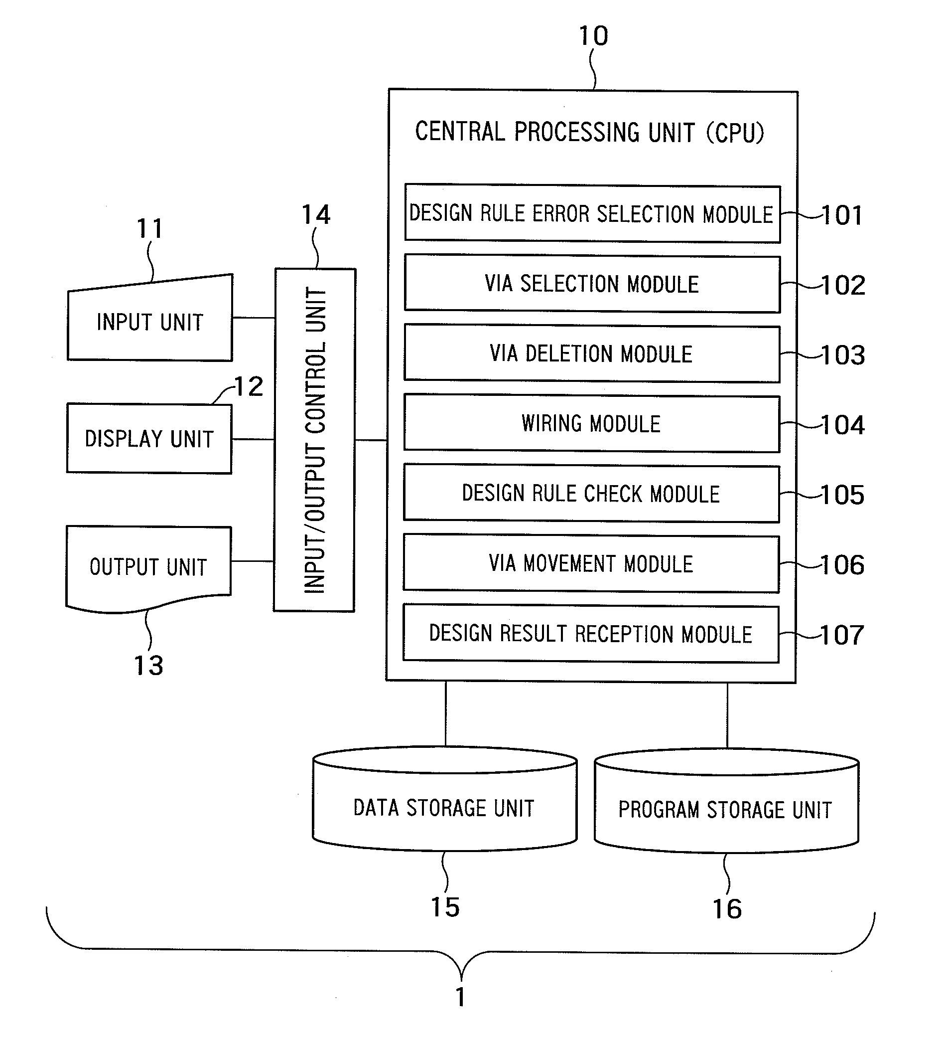
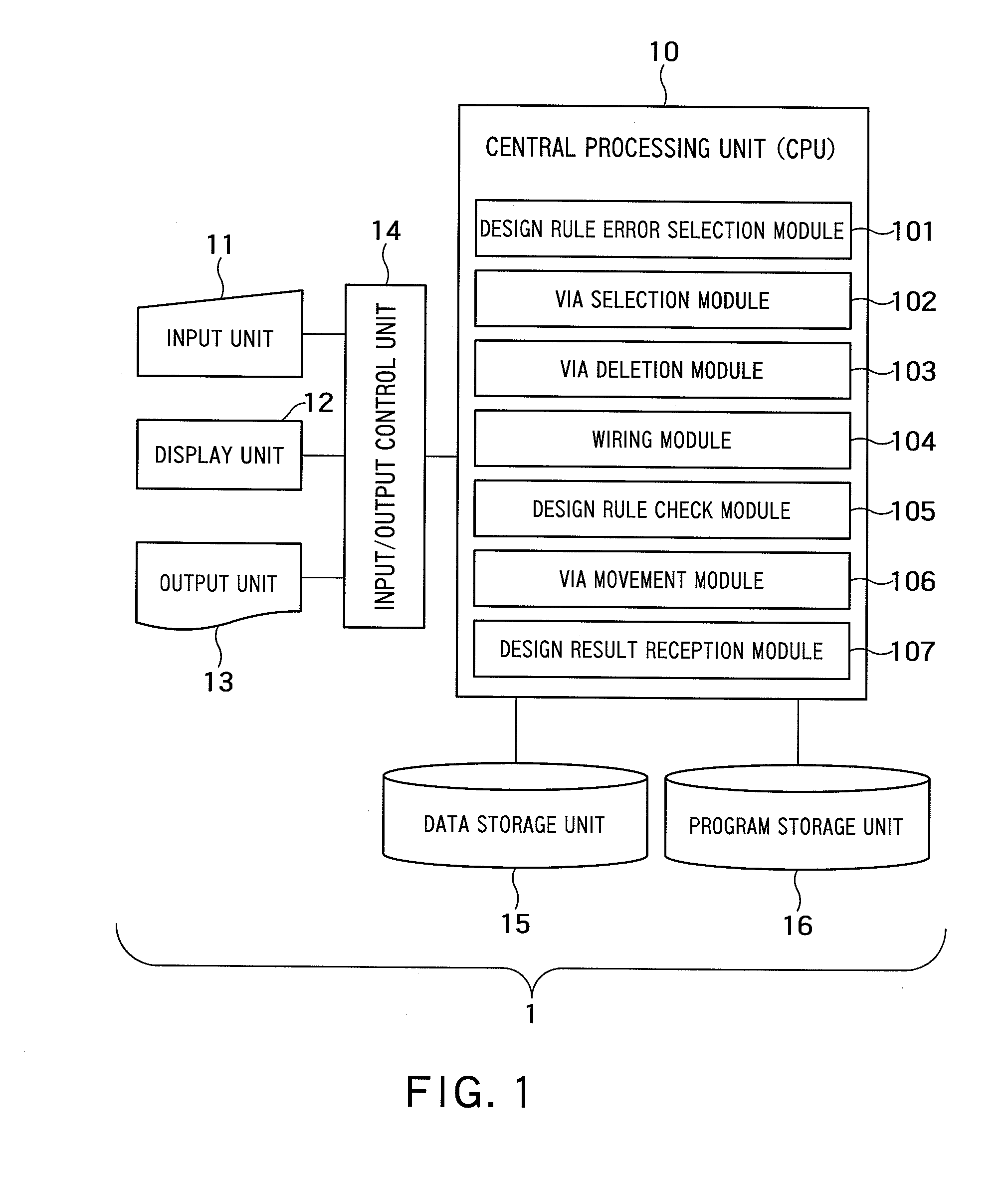
[0065]An automatic design apparatus 1 according to a first embodiment of the present invention comprises an input unit 11 to which input data is supplied, a central processing unit (CPU) 10 which carries out wiring design, a display unit 12 and an output unit 13 which design results are displayed on and provided to, a program storage unit 16 which stores a wiring design program, and a data storage unit 15 which stores various types of data about wiring design, as shown in FIG. 1. The input unit 11, the display unit 12, and the output unit 13 are connected through an input / output control unit 14 to the CPU 10, while the program storage unit 16 and the data storage unit 15 are directly connected to the CPU 10. The CPU 10 comprises a design rule error selection module 101, a via selection module 102, a via deletion module 103, a wiring module 104, a design rule check module 105, a via movement module 106, and a wiring design result reception module 107. These modules will be used by a ...

second embodiment

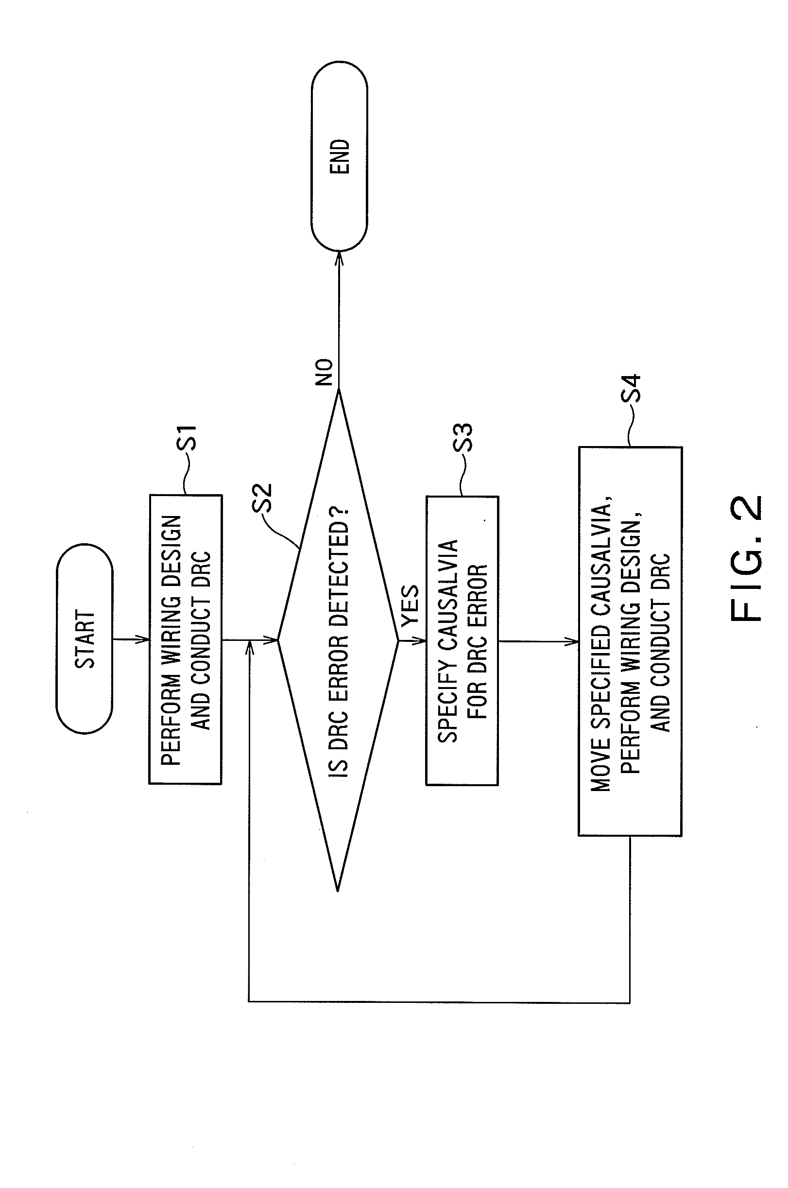
[0102]A description will be given of a second embodiment. In the second embodiment, step 2 (step of specifying causal vias) has been improved. At step 2 in the first embodiment, based on the presumption that all of vias 22 on a wiring board 28 are the possible causal via for design rule errors, those vias have been deleted one by one, repeatedly. In contrast, at step 2 in the second embodiment, the possible causal vias 22 for design rule errors are limited beforehand and then deleted one by one, repeatedly. This gives the second embodiment an advantage of shortening the time to specify the causal vias as compared to the first embodiment.

[0103]More specifically, in the second embodiment, the possible causal vias 22 for a selected design rule error are previously limited to those that are presumed to be present in a range distant by a predetermined distance from the position of the selected design rule error (for example, they are limited to those vias 22 that are to be deleted becaus...

third embodiment

[0106]A description will be given of a third embodiment. In the first embodiment, a causal via has been specified based on the presumption that one causal via 22 corresponds to one design rule error. However, actually, the one-to-one correspondence does not always hold true for the design rule errors and the causal vias; in some cases, one design rule error may be caused by a plurality of the vias 22. Such a situation is accommodated by the third embodiment.

[0107]The wiring design method in the third embodiment is the same as the first embodiment except that step 3-3 in the first embodiment is replaced by step 3-3C. A flow of this design is shown as a flowchart of FIG. 5. A detailed description will be given below only of step 3-3C, which is peculiar to the third embodiment.

[0108](Step 3-3C) A predetermined number of vias 22 are selected from among those in a wiring board 28 as a plurality of selected vias by using a via selection module 102. (The predetermined number may be, for ex...


PUM

PropertyMeasurementUnit
distanceaaaaaaaaaa
distanceaaaaaaaaaa
electricallyaaaaaaaaaa

Abstract

A wiring design method for a wiring board comprises, if design rule errors are found in the wiring design, selecting one of the design rule errors as a selected design rule error, specifying a predetermined number of the second connection terminals as selected second connection terminals that correspond to the selected design rule error, and moving the selected second connection terminals to predetermined coordinate positions. Each time when the selected second connection terminals are moved to the post-movement coordinate positions, the method comprises connecting the second connection terminals and the first connection terminals, conducting the design rule check, and determining whether no design rule errors are detected newly and the selected design rule error is not detected either.

Description

CROSS REFERENCE TO RELATED APPLICATIONS[0001]This application is based upon and claims the benefit of priority from the prior Japanese Patent Application No. 2009-44319, filed on Feb. 26, 2009, the entire contents of which are incorporated herein by reference.BACKGROUND OF THE INVENTION[0002]1. Field of the Invention[0003]The present invention relates to a method for wiring design for a variety of wiring boards such as a wiring board of semiconductor device packages and a printed circuit board (PCB) of electric apparatuses.[0004]2. Background Art[0005]A variety of wiring boards each of which has a plurality of wiring surfaces are available such as a semiconductor package wiring board and a PCB for various electric apparatuses.[0006]For these wiring boards, the wiring design is desired to be of a high integration and a high accuracy. This desire may be accompanied by a tendency of taking a longer time to design the wiring.[0007]Accordingly, to shorten the design time, in the past, a ...

Claims


Application Information

Patent Timeline
Patent Type & Authority Applications(United States)
IPC IPC(8): G06F17/50
CPCG06F17/5077Y10T29/53209Y10T29/53213Y10T29/53178Y10T29/53174Y10T29/53183Y10T29/53217G06F30/394
Inventor NAKANO, MIKIO
Owner KK TOSHIBA
Why Eureka
Try Eureka