Back-contact photovoltaic cell comprising a thin lamina having a superstrate receiver element

Inactive Publication Date: 2010-09-16
GTAT CORPORATION
View PDF9 Cites 56 Cited by
  • Summary
  • Abstract
  • Description
  • Claims
  • Application Information

AI Technical Summary

Benefits of technology

[0005]A first aspect of the invention provides for photovoltaic assembly comprising: a semiconductor lamina having a thickness of 50 microns or less, having a first surface and a second surface, the second surface opposite the first; a receiver element, wherein the semiconductor lamina is bonded to the receiver element at the first surface, with zero, one, or more layers intervening; and a photovoltaic cell, wherein the photovoltaic cell comprises the lamina, and wherein, during normal operation of the photovoltaic cell, current flows into and out of the second surface without current flowing through the first surface.
[0006]Another aspect of the invention provides for a method for f

Problems solved by technology

Making a thinner crystalline cell using conventional methods can be difficult, as thin wafers are prone to breakage.
As will be described, methods of fo

Method used


Image

  • Back-contact photovoltaic cell comprising a thin lamina having a superstrate receiver element
  • Back-contact photovoltaic cell comprising a thin lamina having a superstrate receiver element
  • Back-contact photovoltaic cell comprising a thin lamina having a superstrate receiver element

Examples


example

Amorphous Doped Regions

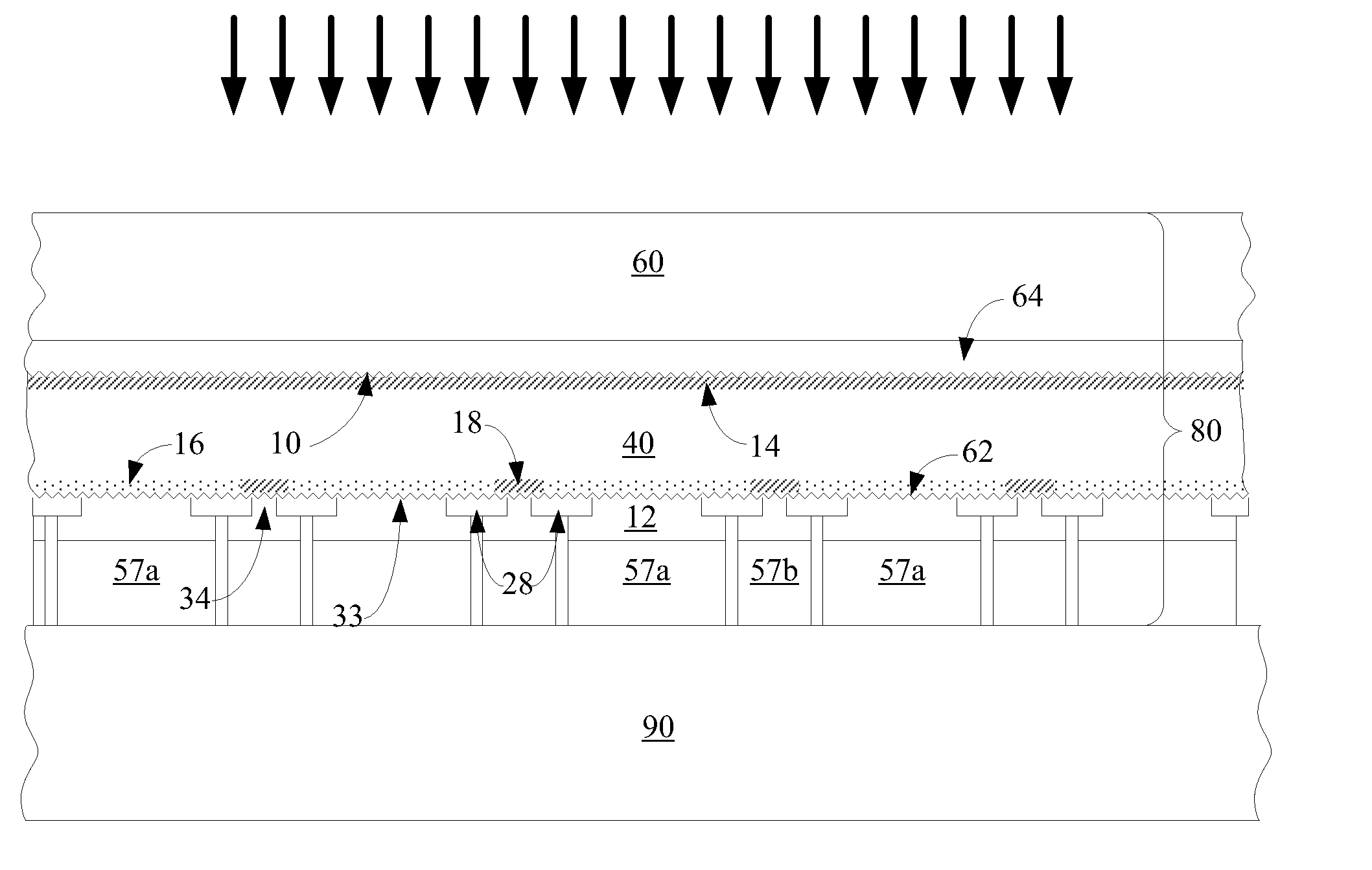
[0052]In an alternative low-temperature embodiment, heavily doped n-type and p-type regions are formed at the back surface of the lamina by depositing heavily doped amorphous silicon. Turning to FIG. 7a, fabrication proceeds as in prior embodiments to the point at which lamina 40, already bonded to receiver element 60, is cleaved from the donor wafer, creating second surface 62. Heavily doped n-type region 14 was previously formed at first surface 10. In this example, lamina 40 is lightly n-doped. FIG. 7a shows receiver element 60 on the bottom, as during fabrication. As in prior embodiments, second surface 62 is optionally textured and treated to remove damage.

[0053]Next a thin layer 72 of intrinsic amorphous silicon may be deposited. This layer serves to passivate second surface 62, and should be thin, for example 50 angstroms or less, for example about 15, 20, or 30 angstroms. In some embodiments, amorphous intrinsic layer 72 may be omitted.

[0054]A layer 74...


PUM


Abstract

A photovoltaic assembly comprises a thin semiconductor lamina and a receiver element, where the receiver element serves as a superstrate in the completed device. The photovoltaic assembly includes a photovoltaic cell. The photovoltaic cell is a back-contact cell; photocurrent passes into and out of the back surface of the cell, but does not pass through the light-facing surface. The lamina is typically substantially crystalline and has a thickness less than about 100 microns, in some embodiments 10 microns or less.

Description

BACKGROUND OF THE INVENTION[0001]The invention relates to a photovoltaic cell electrically contacted only at its back surface, the photovoltaic cell comprising a thin semiconductor lamina.[0002]In conventional crystalline photovoltaic cells formed from silicon wafers, the cell is generally thicker than actually required by the device. Making a thinner crystalline cell using conventional methods can be difficult, as thin wafers are prone to breakage. A photovoltaic cell includes an emitter and a base; typically one of the emitter or the base is contacted at the light-facing surface, while the other is contacted at the opposite face. As will be described, methods of forming a thin photovoltaic cell may present challenges in making electrical contact to both the light-facing and back surfaces of the photovoltaic cell.[0003]There is a need, therefore, for a thin photovoltaic cell where electrical contact to both the emitter and base regions is readily made.SUMMARY OF THE PREFERRED EMBOD...

Claims


Application Information

Patent Timeline
IPC IPC(8): H01L31/00H01L31/0352
CPCH01L31/03921H01L31/042H01L31/046H01L31/1896Y02E10/547H01L31/1804H01L31/022441H01L31/0682H01L31/0747H01L31/1892Y02P70/50
Inventor ZUNIGA, STEVEN M.PETTI, CHRISTOPHER J.HILALI, MOHAMED M.
Owner GTAT CORPORATION
Why Eureka
Try Eureka