
Optical signal processing device
- Summary
- Abstract
- Description
- Claims
- Application Information
AI Technical Summary
Benefits of technology
Problems solved by technology
Method used
Image

Examples
embodiment 1
Illustrative Embodiment 1
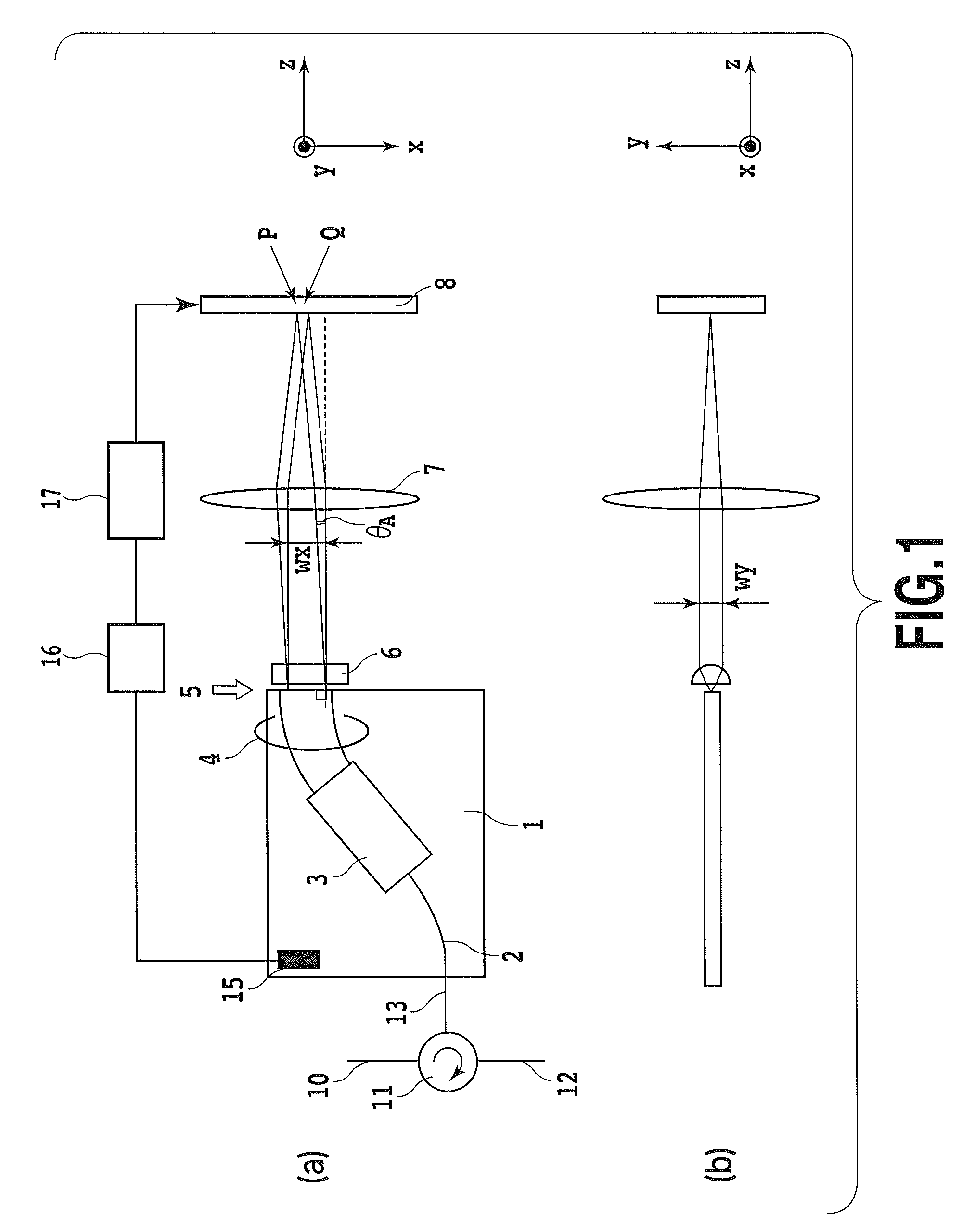
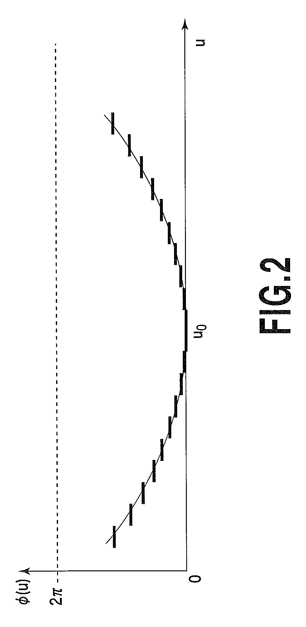
[0033]FIGS. 1(a) and 1(b) illustrate the configuration of an optical signal processing device according to the illustrative embodiment 1 of the present invention. The present invention can be applied to an optical signal processing device that includes a spatial phase control device having a plurality of element devices as a signal processing device. FIG. 1(a) is a top view. FIG. 1(b) is a side view. In the illustrative embodiment 1, the operation will be described by way of a dispersion compensator in which the feature of the present invention can be achieved at the maximum. With reference to FIG. 1(a), the dispersion compensator according to the present invention is composed of: a circulator 11 for inputting and outputting an optical signal; an Arrayed Waveguide Grating 1 (hereinafter referred to as AWG) configuring spatial optical system; a cylindrical lens 6; a focusing lens 7; and a spatial phase control device 8. An inputted optical signal is reflected...
embodiment 2
Illustrative Embodiment 2
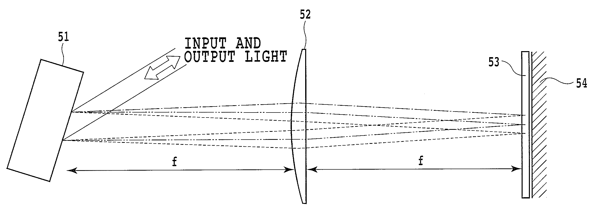
[0062]The dispersion compensator of FIG. 1 that has been described heretofore has a configuration in which a focusing lens is included in the spatial optical system and an optical signal is focused on the spatial phase control device. In this case, the beam diameter on the spatial phase control device as an optical coupling plane may be larger than the pixel repetition cycle of the element device. The present invention also can be applied to an optical signal processing device not including a focusing lens such as a tunable wavelength filter. Even in the case of the optical signal processing device having a configuration not including a focusing lens, it is possible to compensate the temperature dependency of the spectroscopic characteristics of a spectroscopic element such as AWG. Next, the following section will describe an example of an optical signal processing device that uses a spatial phase control device as a signal processing device and that has a f...
PUM
 Abstract
Description
Claims
Application Information