Method of manufacturing color printed circuit board

a technology of printed circuit board and manufacturing method, which is applied in the manufacture of printed circuit boards, printed circuit aspects, solid-state devices, etc., can solve the problems of large increase in size and thickness of sign panels, many man hours and maintenance costs, and difficulty in manufacturing and putting sign panels in place, so as to reduce time and cost of manufacturing.

Inactive Publication Date: 2011-01-06
DGI
View PDF17 Cites 7 Cited by
  • Summary
  • Abstract
  • Description
  • Claims
  • Application Information

AI Technical Summary

Benefits of technology

[0010]The present invention is conceived to solve such problems, and an aspect of the present invention is to provide a method of manufacturing a color printed circuit board, which includes printing an electrically conductive pattern on a flexible board with a conductive ink and printing a color pattern on a light emitting chip mounted on the board using a color ink to exhibit a color, thereby enabling reduction in time and cost for manufacturing the color printed circuit board.

Problems solved by technology

For example, when an electric bulb such as a fluorescent lamp is disposed inside the sign panel, the sign panel significantly increases in size and thickness, thereby making it difficult to manufacture and put the sign panel in place.
Moreover, in this case, since the electric bulb needs to be frequently replaced due to its short lifespan, it consumes many man hours and costs for maintenance.
In the advertisement board using the LED chip, since the LED chip is soldered to a hard printed circuit board, a long time is consumed for soldering.
Further, a number of processes, such as deposition and etching, are performed to form a circuit pattern on the printed circuit board, and post-processes, such as masking and ink printing, for exhibiting a color, must be performed, thereby complicating the process and increasing manufacturing costs.

Method used


Image

  • Method of manufacturing color printed circuit board
  • Method of manufacturing color printed circuit board
  • Method of manufacturing color printed circuit board

Examples


Embodiment Construction

[0019]Embodiments of the invention will now be described in detail with reference to the accompanying drawings. It should be noted that the drawings are not to precise scale and may be exaggerated in thickness of lines or sizes of components for descriptive convenience and clarity only. Furthermore, the terms as used herein are defined by taking functions of the invention into account and can be changed according to the custom or intention of users or operators. Therefore, definition of the terms should be made according to the overall disclosure set forth herein.

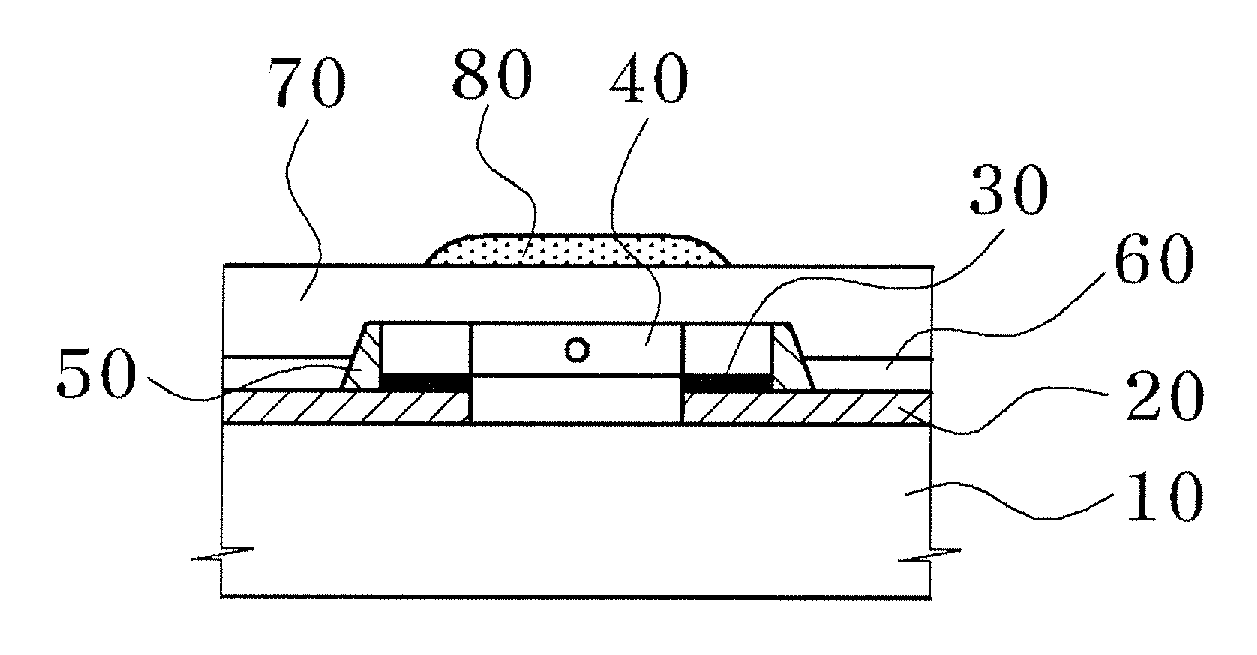
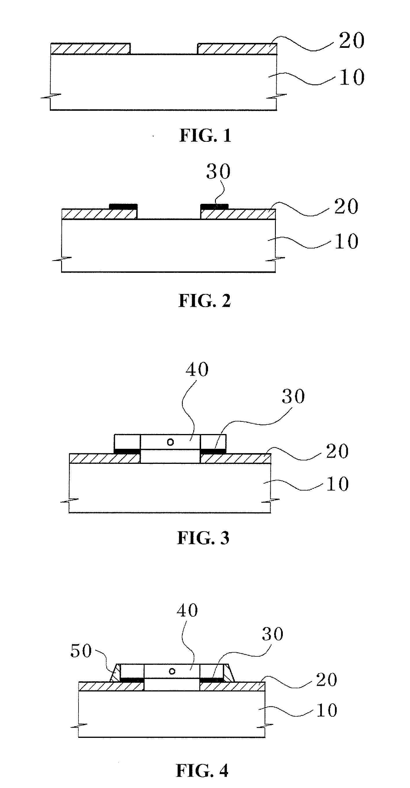
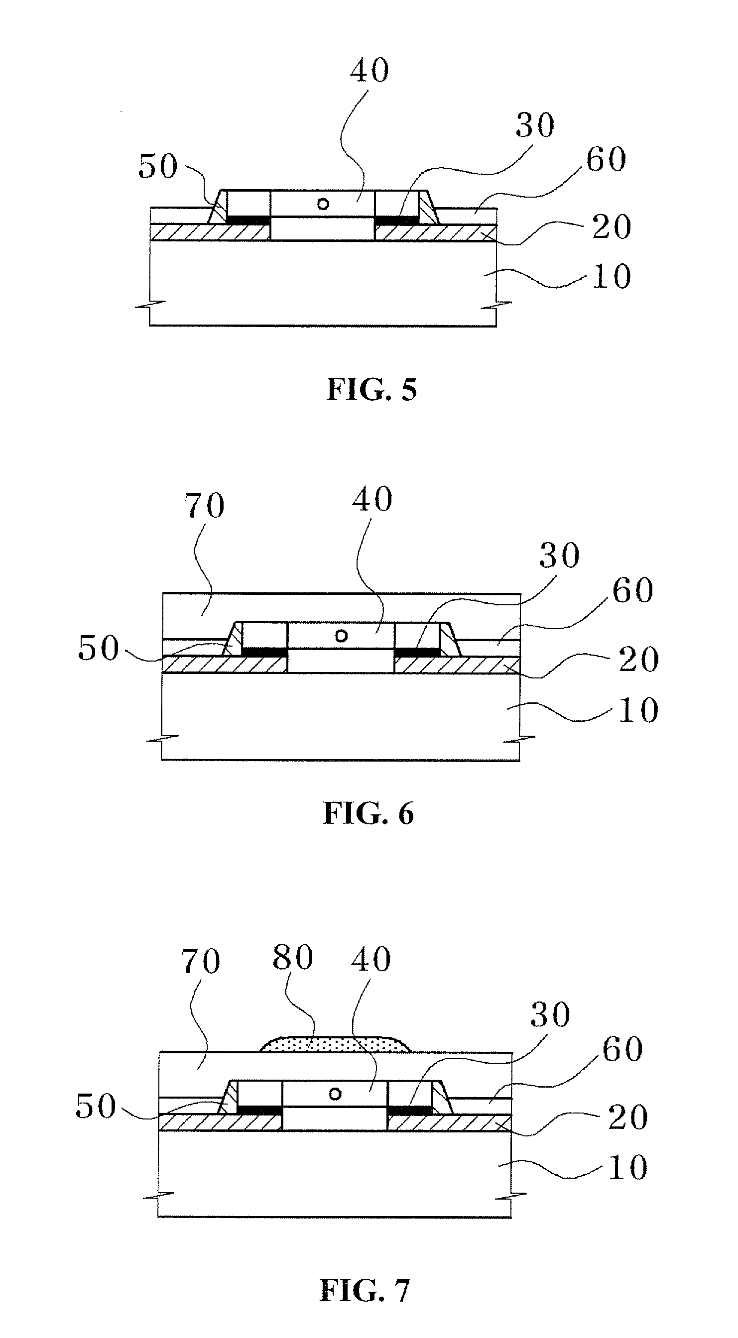
[0020]FIGS. 1 to 7 are sectional views sequentially illustrating a method of manufacturing a color printed circuit board in accordance with an embodiment, and FIG. 8 is a plan view of a color printed circuit board in accordance with an embodiment.

[0021]First, referring to FIG. 1, a conductive ink is non-consecutively printed on a flexible insulation board 10 in a piezoelectric inkjet manner to form an electrically conductiv...


PUM


Abstract

Disclosed herein is a method of manufacturing a color printed circuit board. The method includes non-consecutively printing a conductive ink on a flexible insulation board in a piezoelectric inkjet manner to form an electrically conductive pattern, applying an electrically conductive bonding agent to a light emitting chip mounting portion of the electrically conductive pattern for mounting a light emitting chip, forming a waterproof layer on an overall surface of a resultant after mounting the light emitting chip on the light emitting chip mounting portion of the electrically conductive pattern to which the electrically conductive bonding agent is applied, and forming a color pattern on an overall surface of the light emitting diode using a color ink.

Description

CROSS-REFERENCE TO RELATED APPLICATION[0001]This application claims the benefit under 35 U.S.C. §119(a) of Korean Patent Application No. 10-2009-0061237, filed on Jul. 6, 2009, which is hereby incorporated by reference in its entirety.FIELD OF THE INVENTION[0002]The present invention relates to a method of manufacturing a color printed circuit board and, more particularly, to a method of manufacturing a color printed circuit board, which includes printing an electrically conductive pattern on a flexible board with a conductive ink and printing a color pattern on a light emitting chip mounted on the board using a color ink to exhibit a color, thereby enabling reduction in time and cost for manufacturing the color printed circuit board.DESCRIPTION OF THE RELATED ART[0003]Traffic signboards, information panels, advertisement boards, or the like are printed or painted with desired information to be imparted to road users, and provided with lighting to illuminate the printed or painted i...

Claims


Application Information

Patent Timeline
Patent Type & Authority Applications(United States)
IPC IPC(8): H01L33/62H01L33/48
CPCH01L25/0753H01L33/44H01L33/46H01L33/486H01L33/62H05K3/284H01L2924/0002H05K3/321H05K2201/10106H05K2203/1322H01L2924/00H01L33/00
Inventor CHOI, KWAN SOO
Owner DGI
Why Eureka
Try Eureka