Calibrating device, mapping method and compensation method using the same

a compensation method and image sensor technology, applied in the field of image sensor compensation method, mapping method and compensation method, can solve problems such as discontinuous scan, poor scan, non-uniform gap, etc., and achieve the effect of improving the scan resul

Active Publication Date: 2011-01-13
MICROTEK INT
View PDF13 Cites 0 Cited by
  • Summary
  • Abstract
  • Description
  • Claims
  • Application Information

AI Technical Summary

Benefits of technology

[0006]There are lots of factors may result in poor scan result. Take the scanner with the CIS for instance, some inaccuracy, such as tolerances in a packaging process of the CIS, may result in non-uniform gaps between the CISs, and then discontinuous dispositions of the CISs result in a discontinuous scan result. Therefore, the present invention provides a calibrating device for gaps between image sensors and a mapping method using the same to improve the scan result by using a pattern of the calibrating device and a calculation to determine positions and sizes of the gaps between the image sensors, so as to compensate the scan result according to the positions and the sizes of the gaps.

Problems solved by technology

There are lots of factors may result in poor scan result.
Take the scanner with the CIS for instance, some inaccuracy, such as tolerances in a packaging process of the CIS, may result in non-uniform gaps between the CISs, and then discontinuous dispositions of the CISs result in a discontinuous scan result.
In addition, all gaps, comprising shift gaps along an arrangement line of image sensors and alignment gaps offsetting the image sensors from the arrangement line, result in the discontinuous scan result.

Method used


Image

  • Calibrating device, mapping method and compensation method using the same
  • Calibrating device, mapping method and compensation method using the same
  • Calibrating device, mapping method and compensation method using the same

Examples


Embodiment Construction

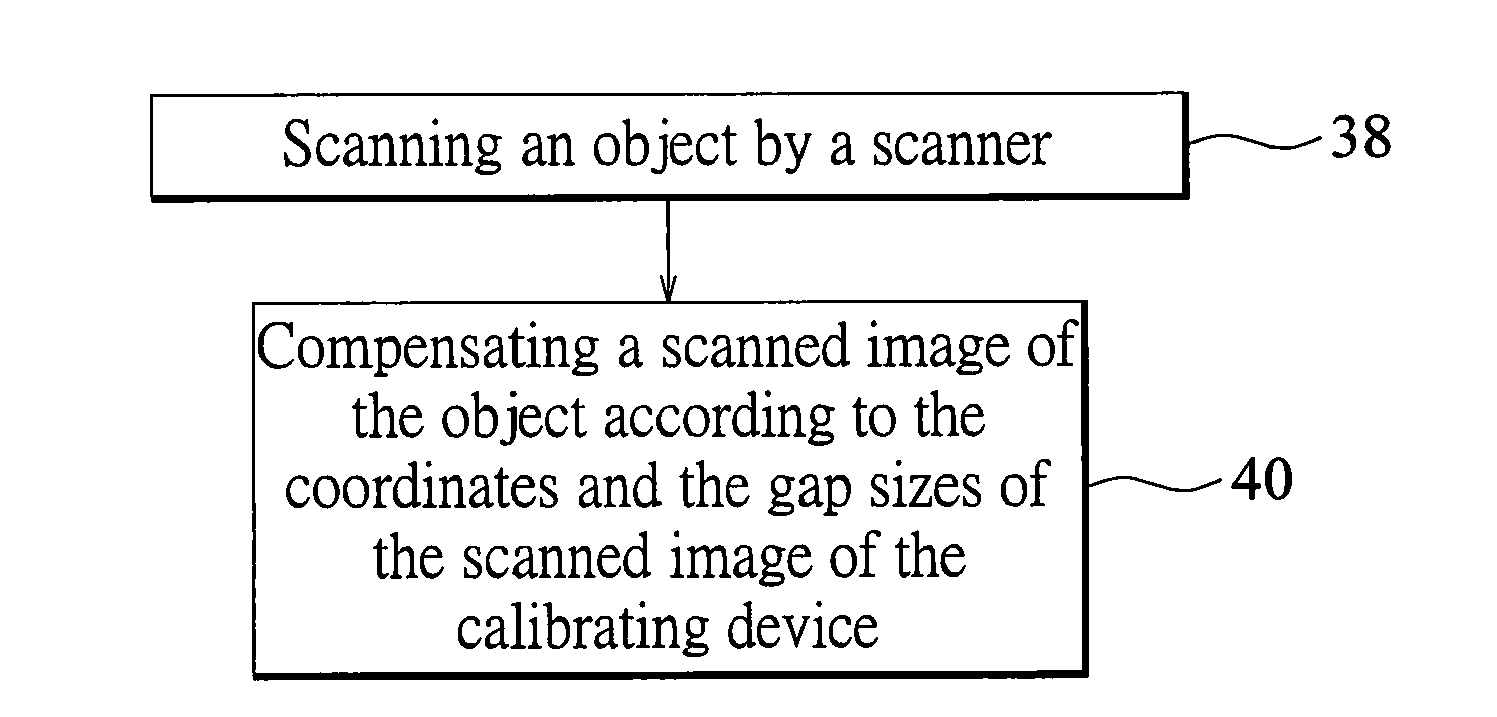
[0017]Reference will now be made in detail to specific embodiments of the present invention. Examples of these embodiments are illustrated in the accompanying drawings. While the invention will be described in conjunction with these specific embodiments, it will be understood that it is not intended to limit the invention to these embodiments. In fact, it is intended to cover alternatives, modifications, and equivalents as may be included within the spirit and scope of the invention as defined by the appended claims. In the following description, numerous specific details are set forth in order to provide a through understanding of the present invention. The present invention may be practiced without some or all of these specific details. In other instances, well-known process operations are not described in detail in order not to obscure the present invention.

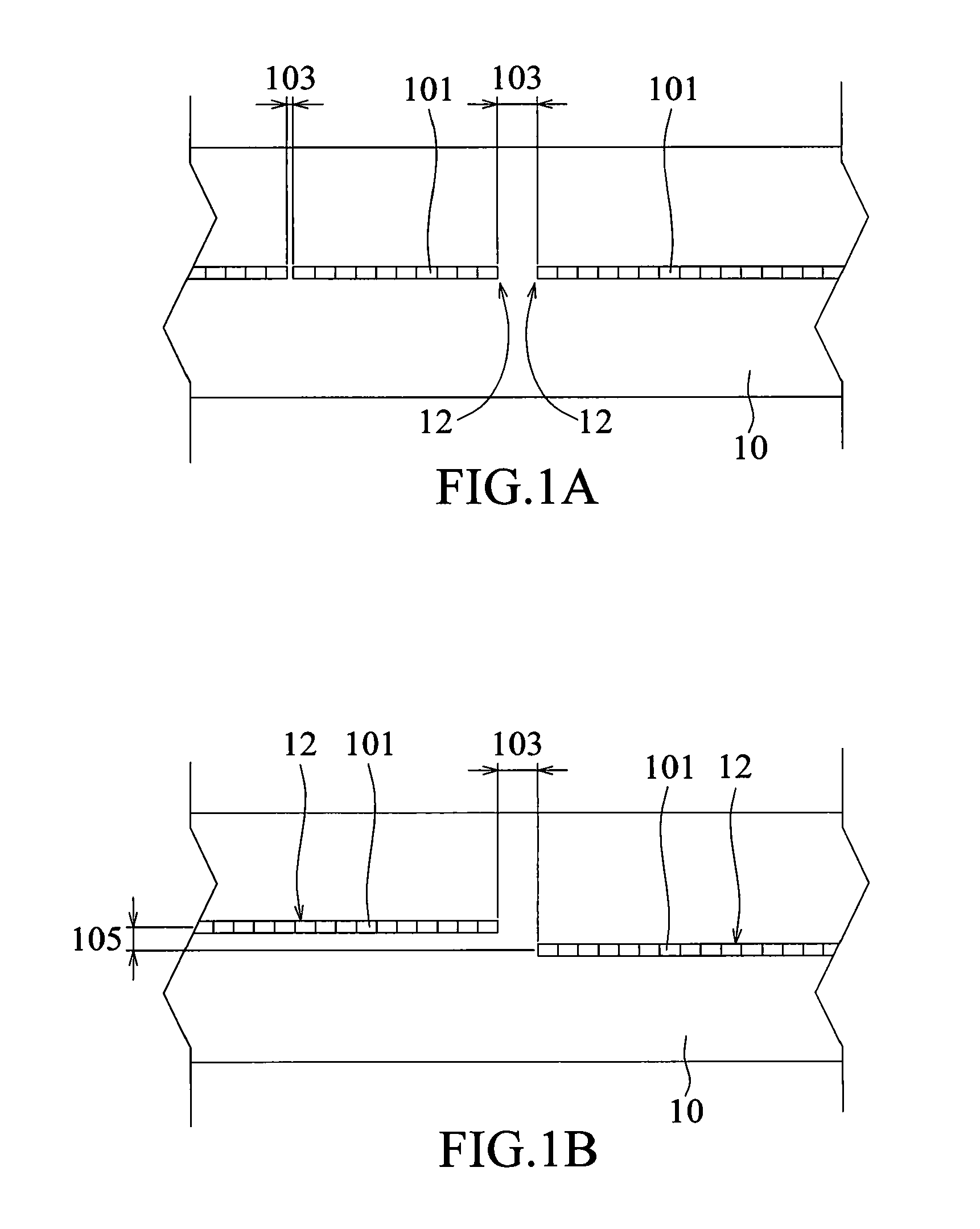
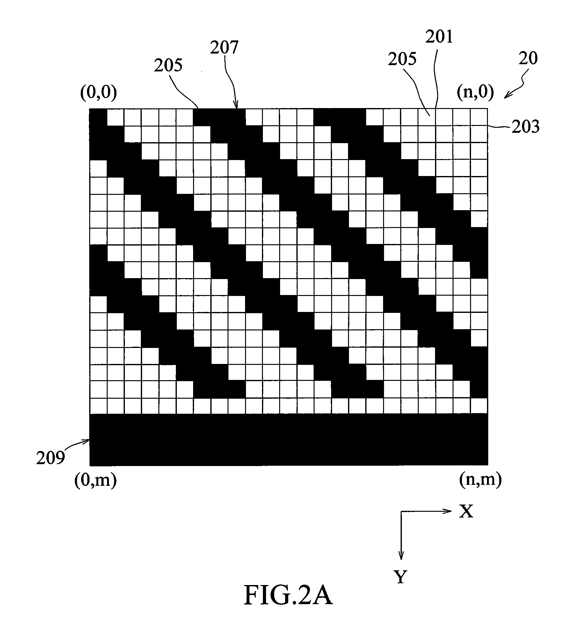
[0018]FIG. 1A illustrates an image sensor arrangement for illustrating a calibrating device and a method for compensating a ...


PUM


Abstract

A calibrating device including a pixel unit array and a pattern is provided. The pixel unit array comprises parallel warp lines and parallel weft lines. Each warp line crosses each weft line to define pixel units all over the pixel unit array. The pattern comprises some pixel units having a gray level different from a gray level of remainder pixel units in the pixel unit array. The pattern comprises spaced bars parallel to one another and not parallel to the warp lines and the weft lines. A characteristic of the pattern is utilized to define target pixel units and comparison pixel units, and the comparison procedure is implemented with the characteristic of the pattern. Positions and gap sizes of gaps between image sensors are mapped out by comparing the target pixel units with the comparison pixel units. The quality of a scanned image is improved with compensation for the gaps.

Description

FIELD OF THE INVENTION[0001]The present invention generally relates to a calibrating device for an image sensor, a mapping method and a compensation method using the same, and more particularly to a calibrating device for a contact image sensor, a mapping method and a compensation method using the same.DESCRIPTION OF THE RELATED ART[0002]Image sensors used in scanners today mainly include charge-coupled device (CCD), contact image sensor (CIS), photomultiplier tube (PMT) and complementary metal oxide semiconductor (CMOS), wherein the CCD and the CIS are widely used in scanners.[0003]In general, the CCD converts light into analog voltage signals and marks up grayscales of each pixel, and then an analog / digital converter converts the analog voltage signals into digital signals. Light provided by a light source must be reflected by mirrors and focused by optical lenses in an imaging process, thus the optical devices increase the total manufacturing cost of the scanner, and the light ne...

Claims


Application Information

Patent Timeline
Patent Type & Authority Applications(United States)
IPC IPC(8): H04N1/04
CPCH04N1/00002H04N1/00013H04N1/00031H04N1/00045H04N1/00053H04N1/1934H04N1/00087H04N1/0009H04N1/0313H04N1/193H04N1/00063
Inventor YU, WAN-JHANG
Owner MICROTEK INT
Why Eureka
Try Eureka