Display device with improved sensing mechanism

a technology of sensing mechanism and display device, which is applied in the field of display device, can solve the problems of not always providing accurate, and achieve the effect of improving the reliability of sensing function

Active Publication Date: 2011-01-20
SAMSUNG DISPLAY CO LTD
View PDF1 Cites 36 Cited by
  • Summary
  • Abstract
  • Description
  • Claims
  • Application Information

AI Technical Summary

Benefits of technology

The present invention provides a display device having improved sensing function reliability and a manufacturing method thereof.
According to an exemplary embodiment of the present invention, an infrared sensing transistor, a visible light sensing transistor, and a readout transistor are simultaneously formed with a top gate structure, and the semiconductor layer is formed of a material that is sensitive to infrared rays such that the number of manufacturing processes and the manufacturing cost may be reduced.
Also, the channel passivation layer is formed on the infrared sensing transistor, and the visible light sensing transistor and the readout transistor are formed on the semiconductor layer, such that the characteristics of the transistor may be improved.
Further, the infrared sensing transistor and the visible light sensing transistor have the top gate structure and the readout transistor has the bottom gate structure such that the photosensitivity of the infrared sensing transistor and the visible light sensing transistor may be improved, and the processing speed of the readout transistor may be simultaneously improved, and thereby the semiconductor layer may be appropriate for the objects of the infrared ray sensing, the visible ray sensing, and the control thereof.

Problems solved by technology

Although conventional sensing devices are available, they do not always provide accurate results because they typically achieve the sensing function or the image sensing function by detecting physical changes.

Method used


Image

  • Display device with improved sensing mechanism
  • Display device with improved sensing mechanism
  • Display device with improved sensing mechanism

Examples


Embodiment Construction

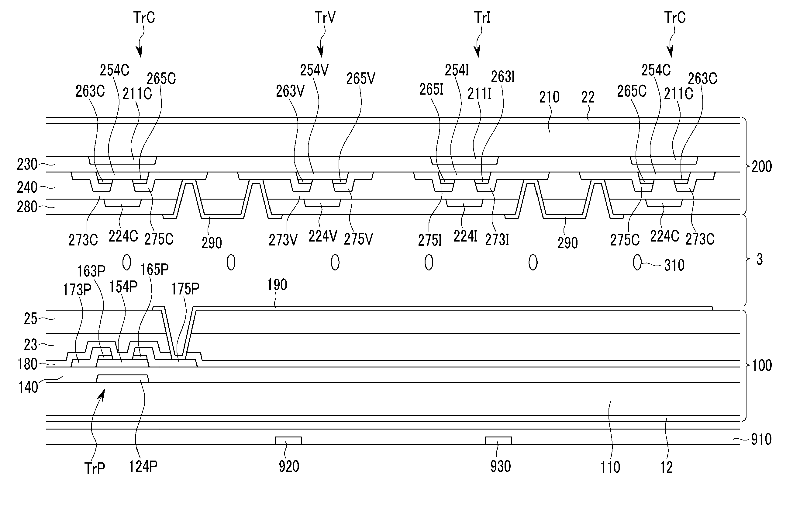
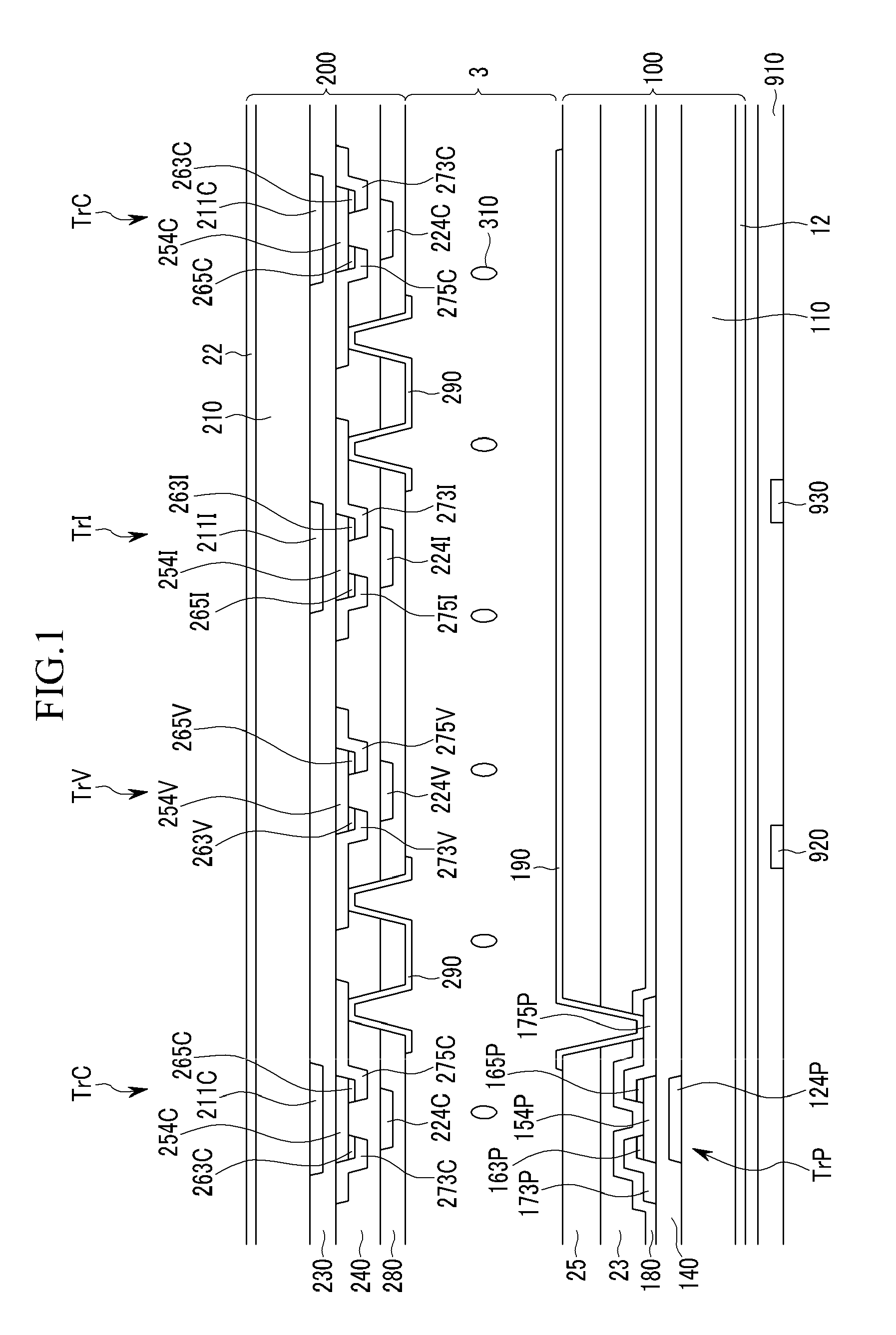
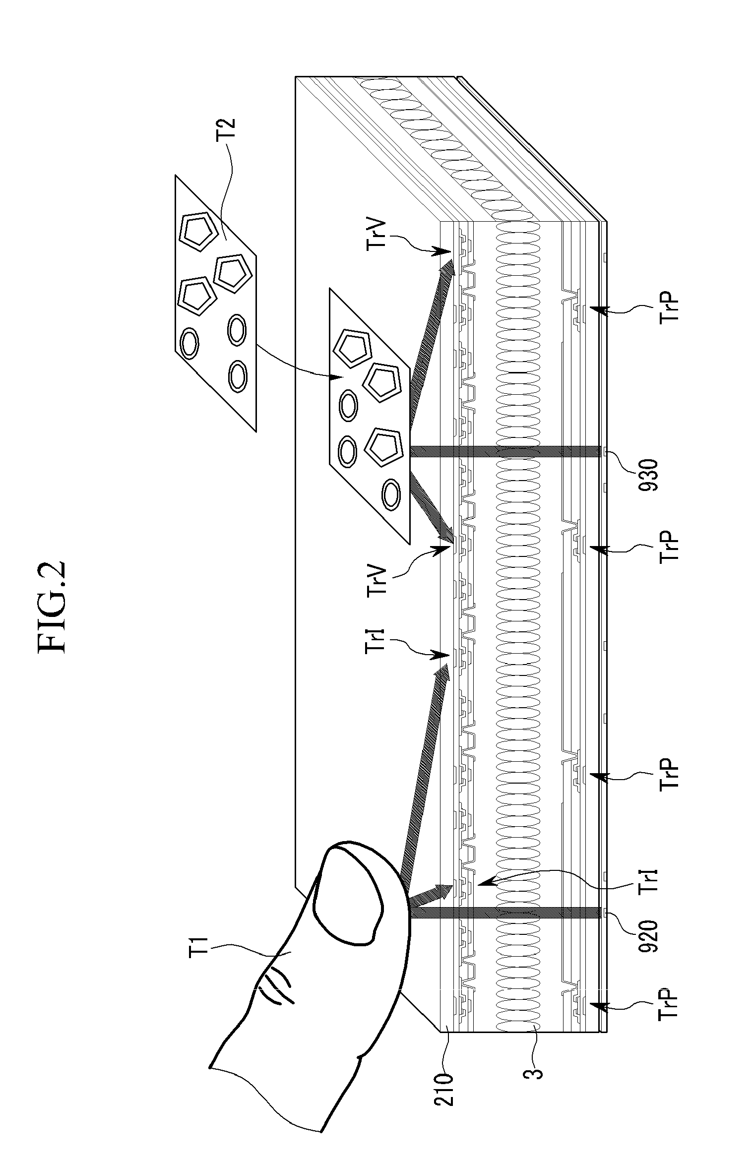
Exemplary embodiments of the present invention will be hereinafter described in detail with reference to the accompanying drawings. The structural shapes, sizes, ratios, numbers, etc. are schematically illustrated in the accompanying drawings such that they may be altered more or less. The drawings are shown from the viewpoint of observation such that the direction or location of explaining the drawings may be variously changed depending upon the position of the observer. Even when reference is made to different elements, like reference numerals may be used to designate those elements. When the terms “include,”“have,”“consist of,” or the like are used, the relevant subject may include other parts unless the term “only” is used to define the contents thereof. When explanation is made by way of a singular term, it may be interpreted in a plural manner as well as in a singular manner. Even when the numerical values, shapes, size comparisons, positional relations, etc. are not explained...


PUM


Abstract

A display panel that includes: a substrate, a sensing transistor disposed on the substrate, and a readout transistor connected to the sensing transistor and transmitting a detecting signal is presented. The sensing transistor includes a semiconductor layer disposed on the upper substrate, a source electrode and a drain electrode disposed on the semiconductor layer, and a gate electrode overlapping the semiconductor layer on the source electrode and the drain electrode. Accordingly, in a display device and a manufacturing method thereof, an infrared sensing transistor, a visible light sensing transistor, and a readout transistor are simultaneously formed with a top gate structure such that the number of manufacturing processes and the manufacturing cost may be reduced.

Description

CROSS-REFERENCE TO RELATED APPLICATIONThis application claims priority to and the benefit of Korean Patent Application No. 10-2009-0065609 filed in the Korean Intellectual Property Office on Jul. 17, 2009, the entire contents of which are incorporated herein by reference.BACKGROUND OF THE INVENTION(a) Field of the InventionThe present invention relates to a display device and a manufacturing method thereof.(b) Description of the Related ArtCurrently, there are many types of flat panel displays being developed. Among them, liquid crystal display is widely used for many applications.Recently, much research has been performed on developing a sensing device that can be used for a liquid crystal display having a touch sensing function or an image sensing function. Although conventional sensing devices are available, they do not always provide accurate results because they typically achieve the sensing function or the image sensing function by detecting physical changes.The above informat...

Claims


Application Information

Patent Timeline
Patent Type & Authority Applications(United States)
IPC IPC(8): H01L33/00
CPCG02F1/13338G02F2001/13312G06F3/042G06F3/0412G02F2203/11G02F1/13312G06F3/0304
Inventor JEON, KYUNG-SOOKYOON, KAP-SOOKIM, WOONG-KWONHAN, SANG-YOUNSONG, JUN-HOYANG, SUNG-HOONCHO, BYEONG-HOONKIM, DAE-CHEOLJEONG, KI-HUNBANG, JUNG-SUK
Owner SAMSUNG DISPLAY CO LTD
Why Eureka
Try Eureka