Semiconductor memory device

Active Publication Date: 2011-07-21
RENESAS ELECTRONICS CORP
View PDF5 Cites 22 Cited by
  • Summary
  • Abstract
  • Description
  • Claims
  • Application Information

AI Technical Summary

Benefits of technology

[0013]A semiconductor memory device according to one invention of the present application comprises: a nonvolatile memory cell having a first field effect transistor included in a first region of a main surface of a semiconductor substrate and a second field effect transistor included in a second region thereof and adjacent to the first field effect transistor.
[0014]The semiconductor memory device further comprises: a first gate electrode of the first field effect transistor formed in the first region; a second gate electrode of the second field effect transistor formed in the second

Problems solved by technology

In the case where writing by a SSI method is performed in a split-gate MONOS memory cell, the occurrence of disturb during writing is a problem.
Therefore, the increase of disturb causes a problem in the split-gate and MONOS-type memory (hereinafter, simply referred to as the MONOS memory) in which writing i

Method used


Image

  • Semiconductor memory device
  • Semiconductor memory device
  • Semiconductor memory device

Examples


first embodiment

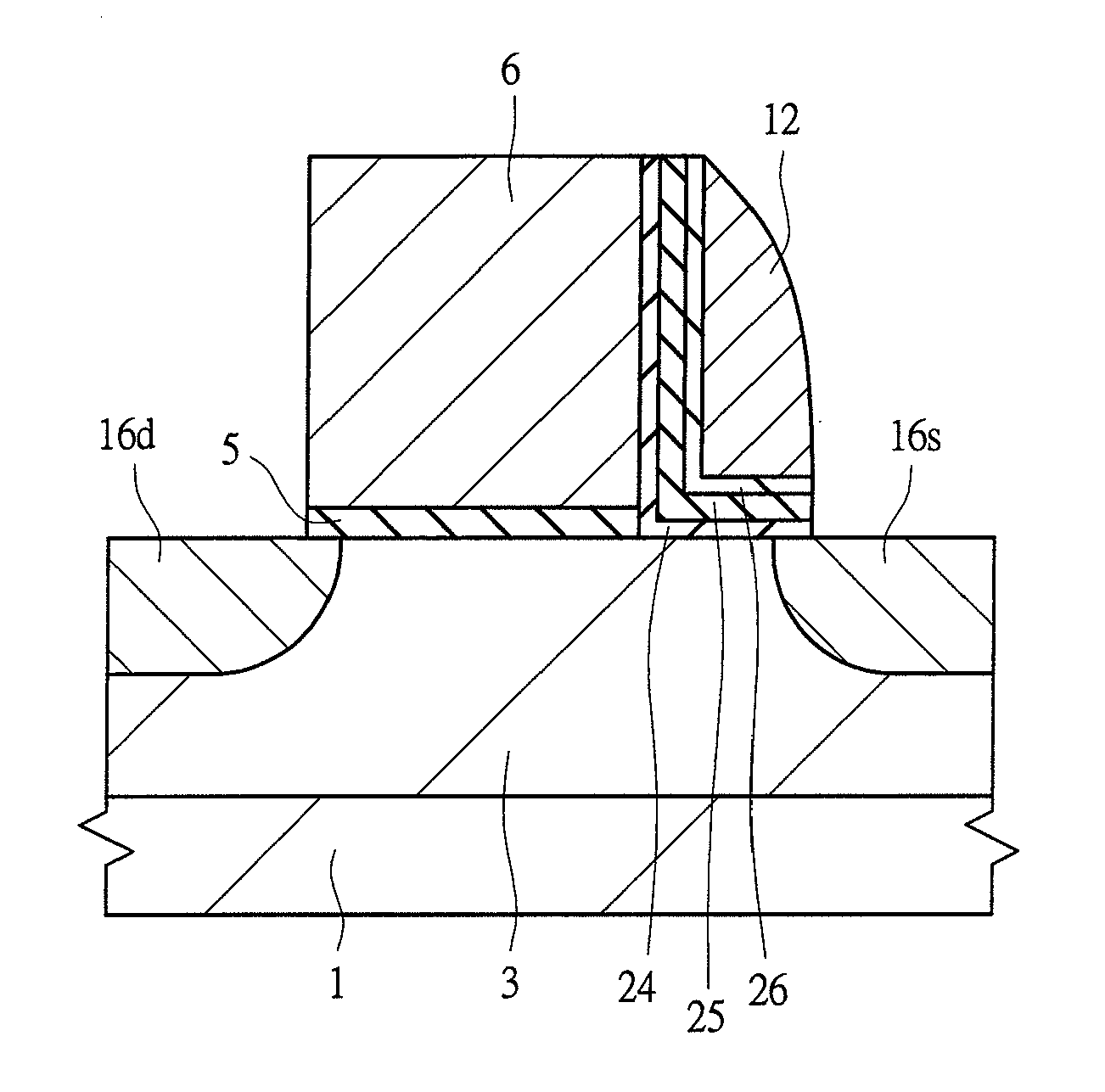
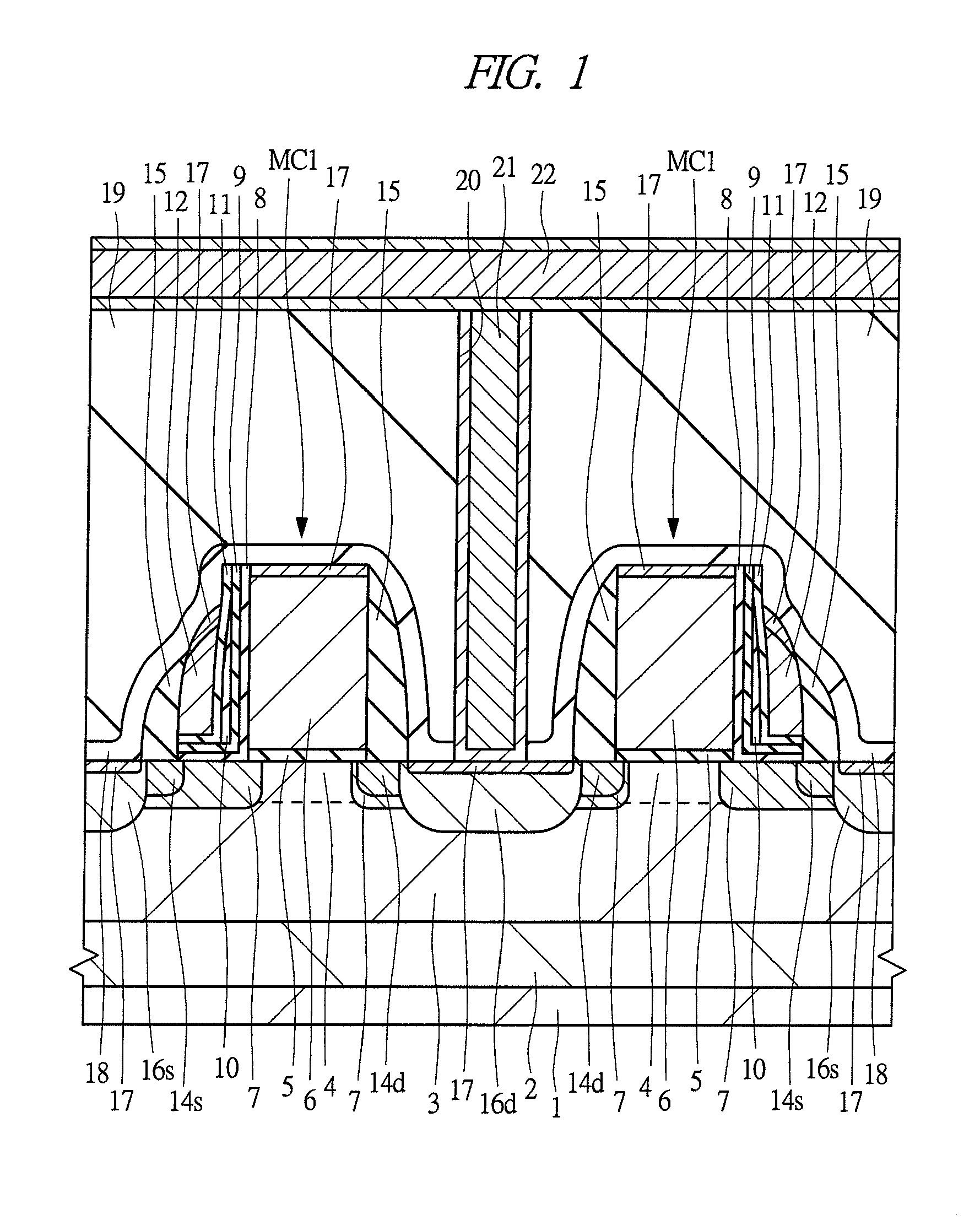
[0052]An example of a structure of a split-gate MONOS memory cell according to the first embodiment of the present invention will be described with reference to FIG. 1. FIG. 1 is a cross-sectional view of the principal part of the split-gate MONOS memory cells obtained by cutting the channels along a line crossing the memory gate electrodes.

[0053]As shown in FIG. 1, a semiconductor substrate 1 is made of, for example, p-type single-crystal silicon, and a p-well 3 containing a p-type impurity implanted therein is formed in an upper portion thereof. In an active region of a main surface (device formation surface) of the semiconductor substrate 1, an nMIS transistor for selecting a memory cell MC1 according to the first embodiment and an nMIS transistor for a memory purpose are disposed. The drain region and source region of each of the memory cells MC1 include relatively low-concentration n−-type semiconductor regions 14d and 14s and relatively high-concentration n+-type source and dr...

second embodiment

[0124]In the second embodiment of the present invention, an example of a manufacturing method of split-gate MONOS memory cells will be described. In the manufacturing method according to the second embodiment, a method of forming the upper-layer insulating films over the memory gate electrodes 12 is different from that of the first embodiment. The manufacturing method of the split-gate MONOS memory cells according to the second embodiment will be described with reference to FIG. 24.

[0125]After the selection gate electrodes 6 are formed as described above with reference to FIG. 16 in the first embodiment, the lower-layer insulating film 8 made of, for example, a silicon oxide film, the charge storage layer 9 made of, for example, a silicon nitride film and an upper-layer insulating film 10b made of, for example, a silicon oxide film are sequentially deposited over the main surface of the semiconductor substrate 1 as shown in FIG. 24. The lower-layer insulating film 8 is formed by an ...


PUM


Abstract

In a semiconductor memory device having split-gate MONOS memory cells, disturb resistance during writing by a SSI method is improved. In addition, with an improvement in the disturb resistance of a non-selected memory cell, a reduction in the area occupied by a memory module can be achieved. Over a side surface of a memory gate electrode, a first insulating film is formed between a charge storage film and a second insulating film so that the total thickness of the first and second insulating films over the side surface of the memory gate electrode is larger than the thickness of the second insulating film under the memory gate electrode.

Description

CROSS-REFERENCE TO RELATED APPLICATION[0001]The present application claims priority from Japanese Patent Application No. 2010-7751 filed on Jan. 18, 2010, the content of which is hereby incorporated by reference to this application.TECHNICAL FIELD OF THE INVENTION[0002]The present invention relates to a semiconductor memory device, and more particularly to a technology effectively applied to a semiconductor memory device having MONOS (Metal Oxide Nitride Oxide Semiconductor) memory cells each using a silicon nitride film or the like as a charge storage layer.BACKGROUND OF THE INVENTION[0003]As electrically writable / erasable nonvolatile semiconductor memory devices, an EEPROM (Electrical Erasable and Programmable Read Only Memory) and a flash memory has been currently used. Each memory cell in the nonvolatile semiconductor memory devices represented by the EEPROM and the flash memory has a charge storage region represented by a conductive floating gate electrode or a trapping insulat...

Claims


Application Information

Patent Timeline
IPC IPC(8): H01L29/792
CPCH01L21/28282H01L29/792H01L29/4234H01L27/11568H01L29/40117H10B43/30
Inventor OKUYAMA, YUTAKA
Owner RENESAS ELECTRONICS CORP
Why Eureka
Try Eureka