Non-volatile semiconductor memory device with intrinsic charge trapping layer
- Summary
- Abstract
- Description
- Claims
- Application Information
AI Technical Summary
Problems solved by technology
Method used
Image

Examples
Embodiment Construction
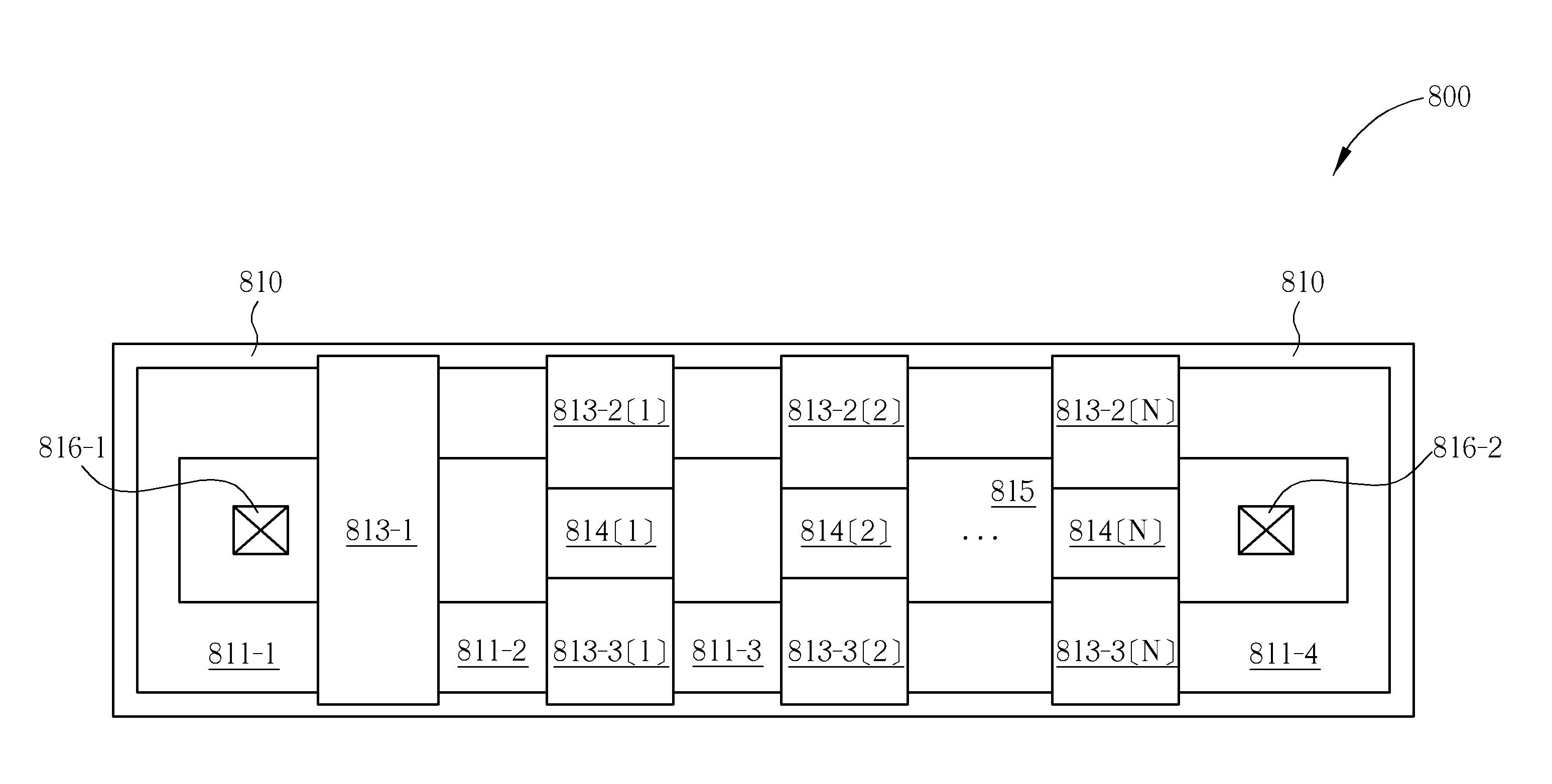
[0023]Please refer to FIG. 3, which is a diagram of a complimentary metal-oxide-semiconductor (CMOS) non-volatile memory cell 300 (hereinafter “the memory cell 300”) according to one embodiment of the present invention. The memory cell 300 may be formed over an active region 315 in a P-well region 310 of a substrate. Although P-well topology CMOS is described, the embodiments described herein are also suitable for application to N-well topology CMOS. A first N+ diffusion region 311-1 may be formed under a first polysilicon gate 313-1, and a second N+ diffusion region may be formed under a second polysilicon gate 313-2 and a third polysilicon gate 313-3.
[0024]The second polysilicon gate 313-2 and the third polysilicon gate 313-3 may be formed a first distance apart from each other. Further, the second polysilicon gate 313-2 and the third polysilicon gate 313-3 may both be formed a second distance apart from the first polysilicon gate 313-1. The first distance and the second distance ...
PUM
 Abstract
Description
Claims
Application Information