Liquid crystal display device

a liquid crystal display and display device technology, applied in non-linear optics, instruments, optics, etc., can solve the problems of difficult restoration, unsatisfactory viewing angle of the display in a specific direction, and difficult to restore, so as to simplify the structure of the electrode and the production process.

Inactive Publication Date: 2011-02-24
JAPAN SCI & TECH CORP
View PDF11 Cites 0 Cited by
  • Summary
  • Abstract
  • Description
  • Claims
  • Application Information

AI Technical Summary

Benefits of technology

[0012]In view of the forgoing, an object of the present invention is to provide a high resolution, wide viewing angle, low power consumption liquid crystal display device which utilizes nematic liquid crystal and which can attain both the memory effect and wide-viewing-angle display characteristic.
[0040]As in the case of ordinary Twisted Nematic (TN) scheme, the above-described twisted planar state can be changed to a homeotropic (vertical alignment) state by means of a pair of surface electrodes which are provided on two substrate surfaces in order to apply an electric field to the liquid crystal layer substantially perpendicular to the substrate surface. However, when the electric field is removed in this state, the liquid crystal transforms to the homogeneous state. Therefore, switching between states can be effected by use of such means for applying a vertical electric field, which is particularly effective for refreshing all pixels of the display.

Problems solved by technology

However, of the aforementioned conventional techniques, notwithstanding its advantages of quick response attributed to ferroelectricity and wide viewing angle attained by use of in-plane switching between two homogeneous alignment states, the former technique in which ferroelectric (chiral smectic C) liquid crystal is used has not yet found wide utility in practice, because of the following problems: the ferroelectric liquid crystal has a layer structure unique to smectic liquid crystal and thus entails difficulty in alignment control as compared to the case of ordinary liquid crystal display devices making use of nematic liquid crystal; and the layer structure, once broken under mechanical impact, is difficult to restore.
Meanwhile, the latter technique in which nematic liquid crystal is combined with alignment layers which have undergone fine grating treatment involves the following problem.
That is, because this technique is based on switching between the two states of homeotropic (vertical) alignment state and hybrid alignment state while making use of flexoelectric effect, unsatisfactory viewing angle of the display arises in a specific direction, because of the hybrid alignment.
However, since liquid crystal material of such high flexoelectric coefficient generally remains unknown, successful reduction in drive voltage and power consumption has not yet been attained.
Thus, this technique also has not yet achieved widespread practical use.
As described above, according to the art known hitherto, liquid crystal displays including nematic liquid crystal, which do not have a layer structure and in which alignment control is easy, encounter difficulty in attaining both low power consumption by virtue of the memory effect and wide viewing angle of the display.

Method used


Image

  • Liquid crystal display device
  • Liquid crystal display device
  • Liquid crystal display device

Examples


first embodiment

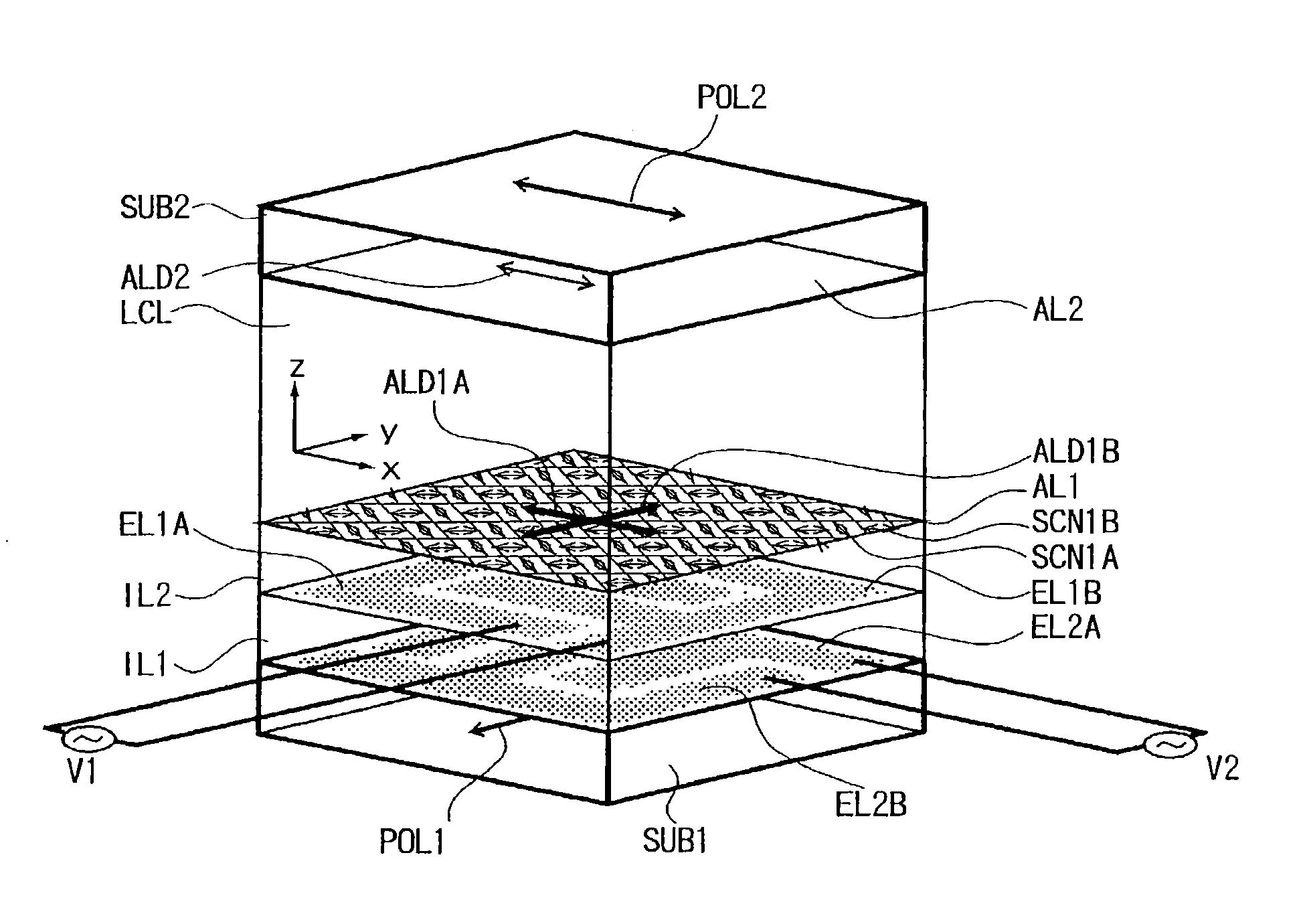
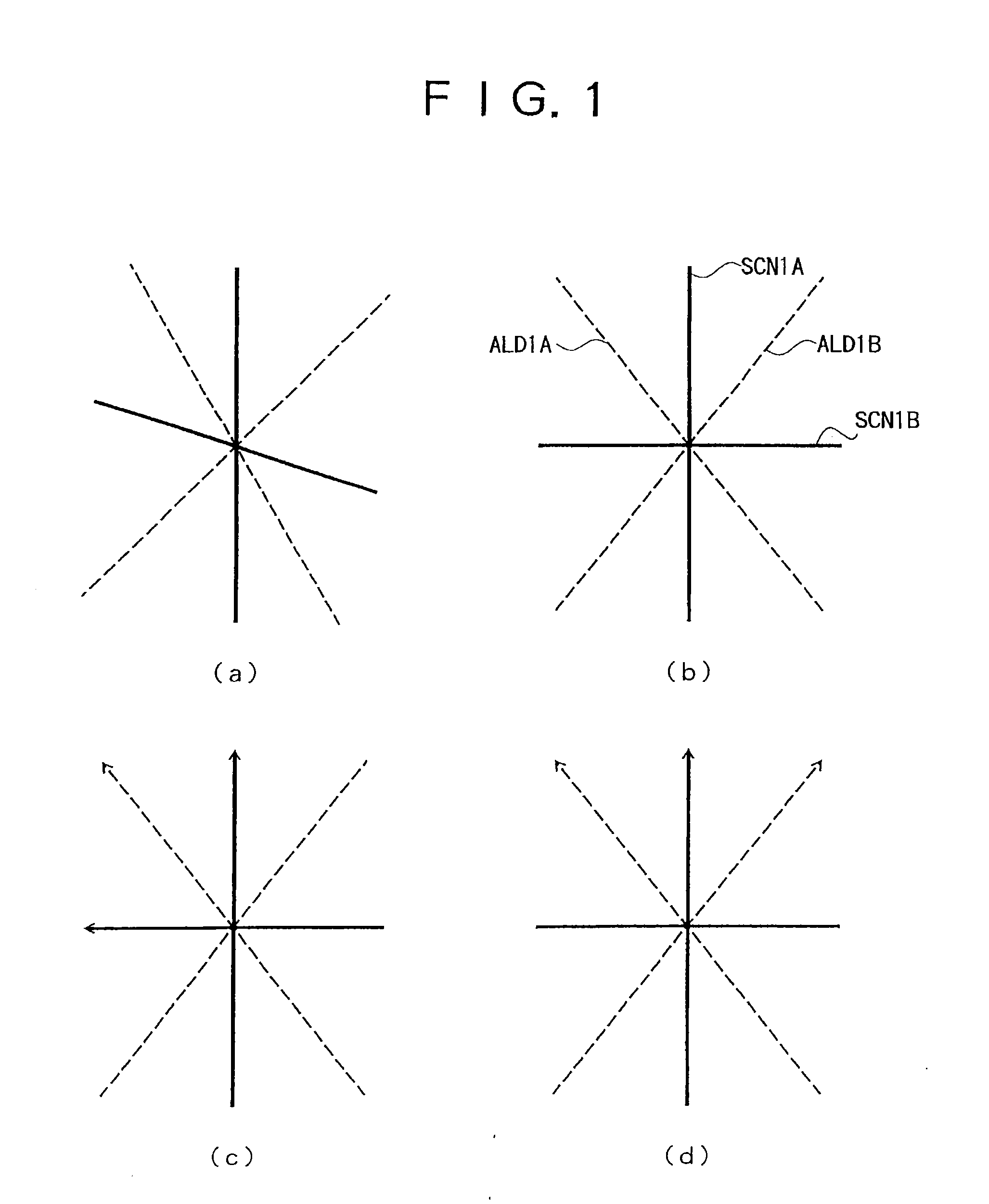
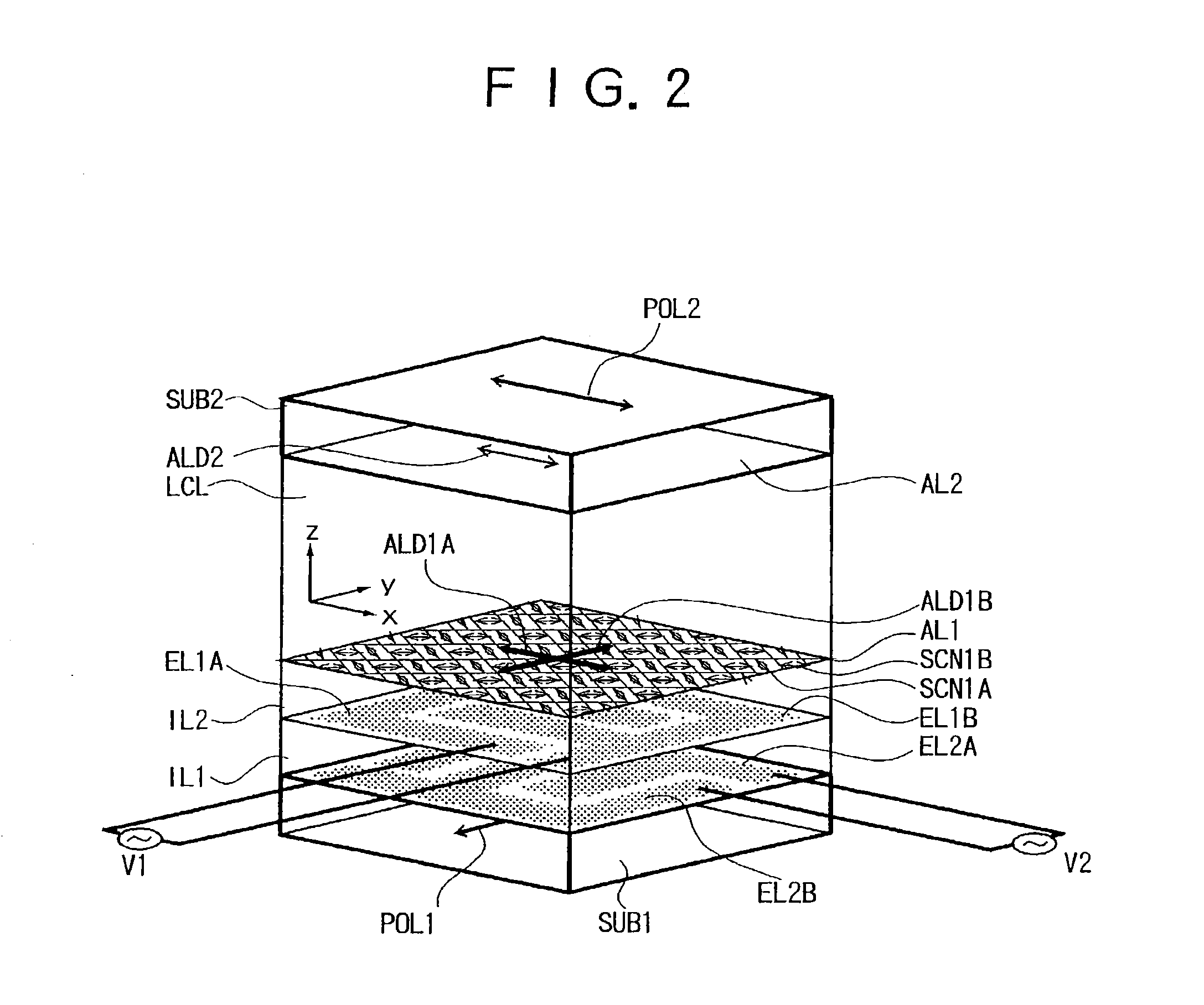
[0053]FIG. 2 is a view showing the configuration of a liquid crystal display device according to the present invention.

[0054]Two transparent glass substrates each having a thickness of 1.1 mm and polished surfaces were used for substrates SUB1 and SUB2 shown in FIG. 2.

[0055]A pair of interdegitated electrodes EL2A and EL2B were formed on the substrate SUB1 through a process of forming a transparent conductive layer of ITO (indium tin oxide) on the substrate and patterning the conductive layer. Subsequently, an insulating protective film IL1 of silicon nitride having a thickness of 600 nm was formed on the electrodes EL2A and EL2B.

[0056]Similarly, another pair of interdegitated electrodes EL1A and EL1B were formed on the insulating film IL1 perpendicular to the electrodes EL2 through a process of forming a transparent conductive layer of ITO on the insulating film IL1 and patterning the conductive layer. Subsequently, an insulating protective film IL2 of silicon nitride having a thic...

second embodiment

[0083]Next, the present invention will be described.

[0084]A liquid crystal display device according to the second embodiment was fabricated in a manner similar to that of the first embodiment, except that a film of a photosensitive materials was formed on one substrate as an alignment layer, and the surface of the film was scanned by use of ultraviolet light; and a liquid crystal composition contained CB-15 of Merck as a chiral dopant and was composed such that the composition had a helical pitch of about 15 μm.

[0085]Specifically, a mixture of diamine compounds containing equimolar amounts of 4,4′-diaminodiphenylmethane and a compound of Formula 1 having a diazobenzen group was treated with an acid anhydride of pyromellitic dianhydride and / or 1,2,3,4-cyclobutantetracarboxylic acid, to thereby form a mixture of polyamic acids. After being applied to the substrate surface, the mixture of polyamic acids was fired at 200° C. for 30 minutes to thereby be imidized. By use of GaN a laser l...

third embodiment

[0090]Next, the present invention will be described.

[0091]A liquid crystal display device according to the third embodiment was fabricated in a manner similar to that of the first embodiment, except that TX2A of Merck was used as a liquid crystal material; as shown in FIG. 7, a single pair of interdegitated electrodes were provided; and a two-frequency drive circuit was used.

[0092]The liquid crystal composition TX2A is a nematic composition whose dielectric anisotropy (Δ∈) becomes positive at low frequency and negative at high frequency and which is therefore suitable for two-frequency drive. The crossover frequency of the liquid crystal composition is 6 kHz.

[0093]FIG. 8 shows a drive waveform and an electro-optic property of the liquid crystal display device according to the present embodiment. As shown in FIG. 8, switching between two states by use of the single pair of interdegitated electrodes could be effected by use of AC voltage V1 which had an amplitude of 8 vpp and a freque...


PUM

PropertyMeasurementUnit
angleaaaaaaaaaa
pre-tilt anglesaaaaaaaaaa
pre-tilt angleaaaaaaaaaa

Abstract

A high resolution, wide viewing angle, low power consumption liquid crystal display device which utilizes nematic liquid crystal and which can attain both the memory effect and wide-viewing-angle display characteristic. A liquid crystal display device that utilizes nematic liquid crystal and includes a pair of transparent substrates; a group of electrodes for applying to a liquid crystal layer disposed between the pair of substrates an electric field having a component substantially parallel to the surfaces of the substrates; and an alignment layer disposed between the liquid crystal layer and at least one of the pair of substrates and having been subjected to liquid crystal anchoring treatments in plural directions. The plurality of liquid crystal anchoring directions of the alignment layer form substantially equal angles relative to one another, and a rising angle in each of the liquid crystal anchoring directions with respect to the corresponding substrate surface is substantially zero.

Description

TECHNICAL FIELD[0001]The present invention relates to a liquid crystal device, and more particularly to a liquid crystal device of low power consumption and high resolution.BACKGROUND ART[0002]Conventionally, as display devices used in portable information terminals such as cellular phones, liquid crystal display devices making use of nematic liquid crystal have mainly been used, by virtue of their low drive voltage and low power consumption characteristics. In association with the recent rapid increase in the use of portable information terminals, the number of such liquid crystal display devices being produced has increased accordingly. At the same time, there has arisen demand for higher display performance, such as an increased number of pixels (characters).[0003]In addition, in view of a desire to lengthen the period of time over which battery-based portable apparatus can be continuously operated, technologies that attain not only the aforementioned higher display functions, in...

Claims


Application Information

Patent Timeline
Patent Type & Authority Applications(United States)
IPC IPC(8): G02F1/141G02F1/1337G02F1/1343G02F1/139
CPCG02F1/133753G02F1/134363G02F1/1391G02F1/1392G02F2001/133749G02F2001/133757G02F1/1337G02F1/133788G02F1/134309G02F1/133749G02F1/133757
Inventor YONEYA, MAKOTOKIM, JONG-HYUNYOKOYAMA, HIROSHIYAMAMOTO, JUN
Owner JAPAN SCI & TECH CORP
Why Eureka
Try Eureka