Plasma arrestor insert

a technology of arrestor and insert, which is applied in the direction of circuit-breaking switch details, circuit-breaking switch for excess current, circuit-breaking switch details, etc., can solve the problems of increasing the cost of ownership, adverse effects, pitting and melting of supply lines, etc., and achieves the effect of plasma generation, and reducing the likelihood of arcing

Active Publication Date: 2011-03-31
LAM RES CORP
View PDF6 Cites 30 Cited by
  • Summary
  • Abstract
  • Description
  • Claims
  • Application Information

AI Technical Summary

Benefits of technology

[0016]It is an object of the present invention to provide a dielectric arrestor insert that decreases the likelihood of arcing and plasma generation in the dielectric arrestor insert.

Problems solved by technology

This produces adverse effects such as pitting and melting of the supply lines.
However, such electrical insulators increase cost of ownership.
If electrical arcing occurs, damage to bowl components can occur.
A problem with this tactic is that decreasing the width d1 and depth d2 of longitudinal channel 212 of dielectric arrestor insert 106 will increase the pressure drop across the components, and that will decrease the amount of helium supplied into wafer processing system 112.
However, arcing or light-up potential can be an issue if the increased length comes in the form of a longer, line-of-site path.
As such, in system 100, this is not a viable option.

Method used


Image

  • Plasma arrestor insert
  • Plasma arrestor insert
  • Plasma arrestor insert

Examples


Embodiment Construction

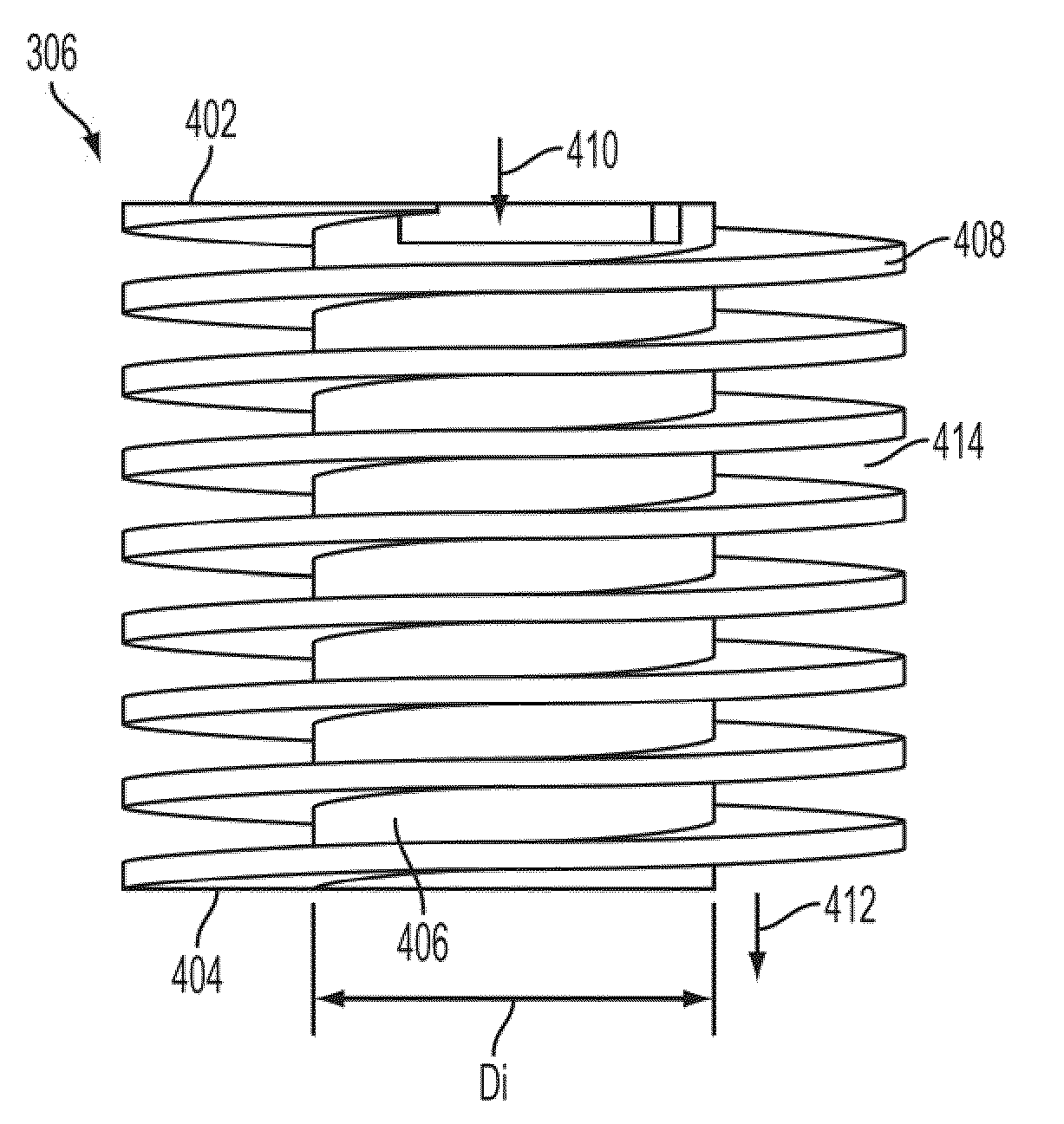
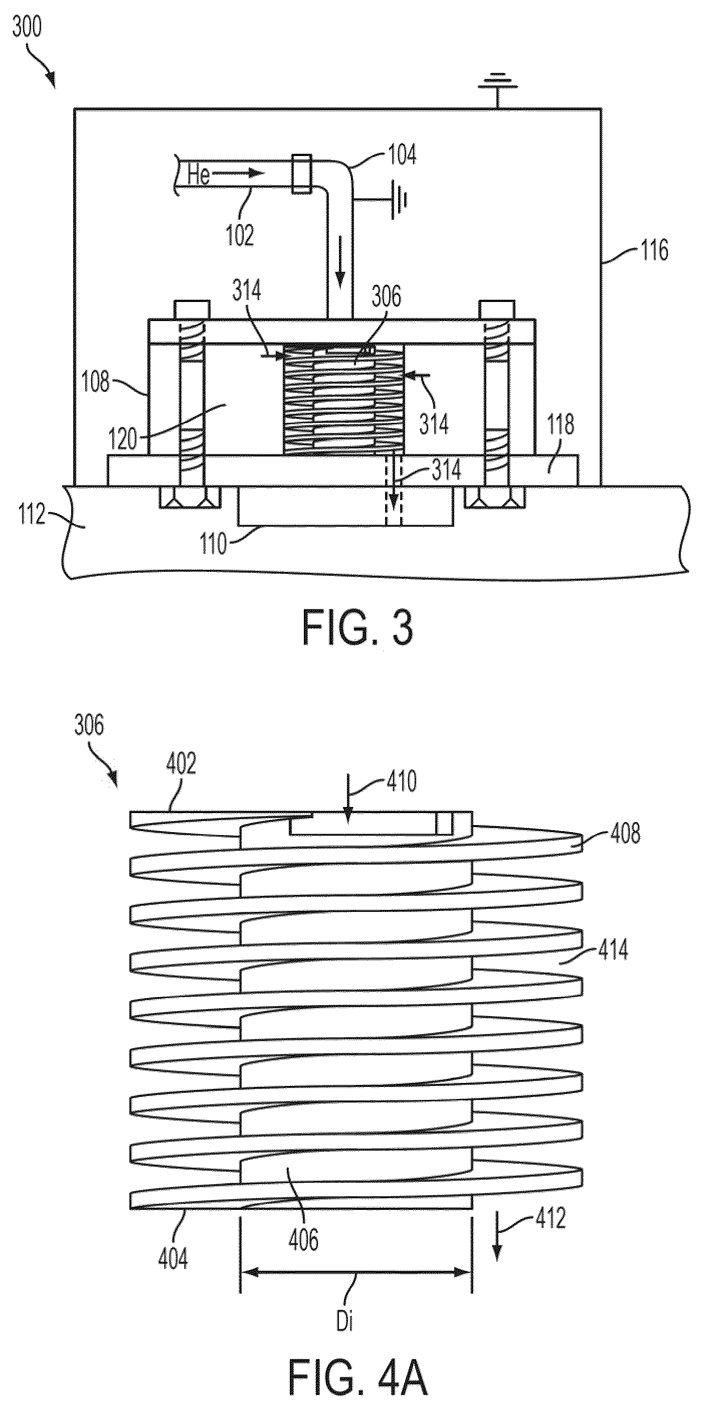
[0036]In a helium supply system that supplies helium to a chamber wafer processing system, a portion of the helium supply system may be at or near ground potential, whereas a portion of the chamber wafer processing system may have a high electrical potential. In such a case, helium within the helium supply line or in the dielectric arrestor insert positioned to supply helium into the chamber wafer processing system has a likelihood of plasma light-up or electrical arcing. In accordance with an aspect of the present invention, the likelihood of helium light-up within the dielectric arrestor insert or arrestor housing is decreased by increasing the length that the helium gas travels in the dielectric arrestor insert. More particular, in accordance with an aspect of the present invention, a dielectric arrestor insert includes non-linear channels into which the helium gas passes. The non-linear channels increase the distance that the helium gas travels in dielectric arrestor insert as c...


PUM


Abstract

A dielectric arrestor insert for use in a chamber wafer processing system having a gas input line, an arrestor housing and a wafer processing space. The input line is able to provide gas to the arrestor housing. The arrestor housing is able to house the dielectric arrestor insert. The dielectric arrestor insert comprises a gas entry portion, a non-linear channel and a gas exit portion. The gas entry portion is arranged to receive the gas from the input line. The non-linear channel is arranged to deliver the gas from the gas entry portion to the gas exit portion. The gas exit portion is arranged to deliver the gas from the non-linear channel to the wafer processing space.

Description

[0001]The present application claims benefit under 35 U.S.C. §119 (e) to U.S. provisional patent application 61 / 165,270, filed Mar. 31, 2009, the entire disclosure of which is incorporated herein by reference.BACKGROUND[0002]The semiconductor manufacturing industry places increased emphasis on cost savings and efficiency to increase a constantly dwindling profit margin. One important effort to drive costs lower is to preserve components within a system that requires extremely high ion energy at the substrate surface when using helium based plasma to complete the required etching process. To create this high ion energy at the substrate surface, a high voltage is applied at the substrate surface, which creates a large electrical field gradient extending back into the helium supply line, which in turn creates unwanted electrical arcing between surfaces and generates plasma in the supply lines and other components. This produces adverse effects such as pitting and melting of the supply ...

Claims


Application Information

Patent Timeline
Patent Type & Authority Applications(United States)
IPC IPC(8): H02H1/00
CPCH01L21/67069
Inventor COMENDANT, KEITH
Owner LAM RES CORP
Why Eureka
Try Eureka