Light-emitting device and method of making the same
- Summary
- Abstract
- Description
- Claims
- Application Information
AI Technical Summary
Problems solved by technology
Method used
Image

Examples
Embodiment Construction
[0022]For to better and concisely explain the disclosure, the same name or the same reference number given or appeared in different paragraphs or figures along the specification should has the same or equivalent meanings while it is once defined anywhere of the disclosure.
[0023]The following shows the description of the embodiments of the present disclosure in accordance with the drawings.
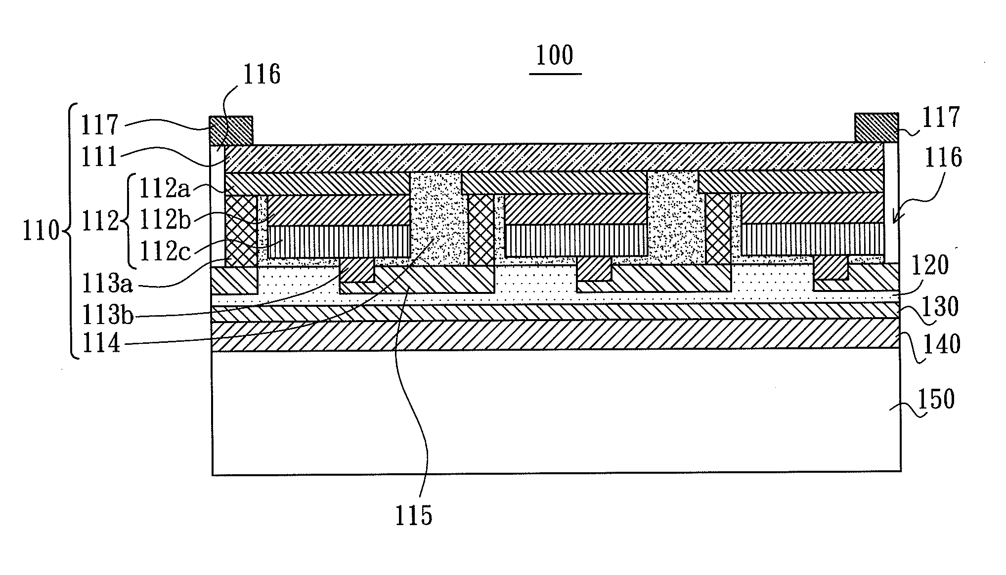
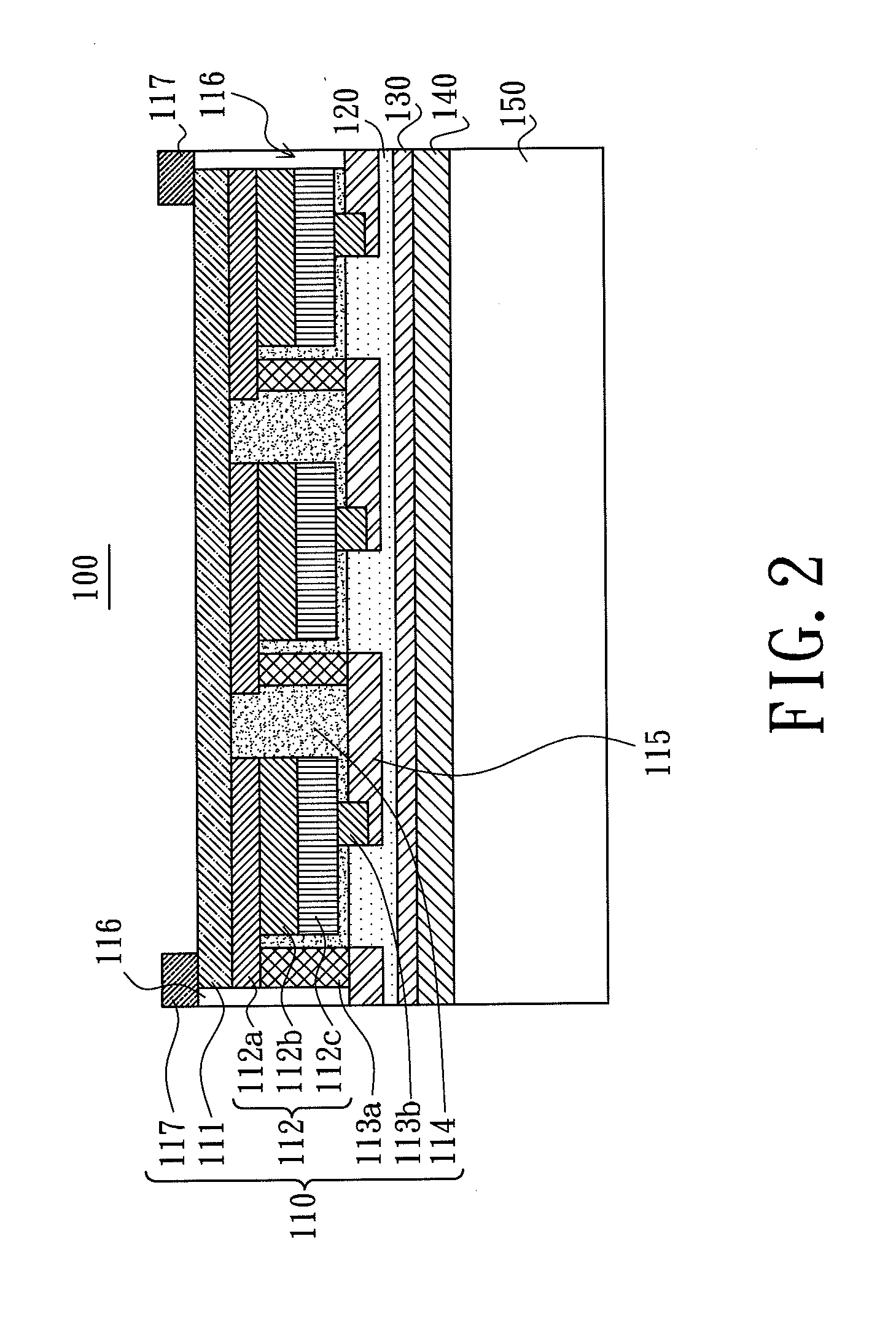
[0024]As shown in FIG. 2, the light-emitting device 100 comprises a light-emitting diode chip 110, an insulating layer 120, a reflective layer 130, a bonding layer 140, and a permanent substrate 150.
[0025]The insulating layer 120 is formed on the light-emitting diode chip 110. The reflective layer 130 is formed on the insulating layer 120 opposite to the light-emitting diode chip 110 for reflecting the light generating from the light-emitting diode chip 110 so as to improve the light extraction efficiency of the light-emitting device 100. The bonding layer 140 is formed on the reflective layer 130 ...
PUM
 Abstract
Description
Claims
Application Information
 - R&D Engineer
- R&D Manager
- IP Professional
- Industry Leading Data Capabilities
- Powerful AI technology
- Patent DNA Extraction
Browse by: Latest US Patents, China's latest patents, Technical Efficacy Thesaurus, Application Domain, Technology Topic.
© 2024 PatSnap. All rights reserved.Legal|Privacy policy|Modern Slavery Act Transparency Statement|Sitemap