

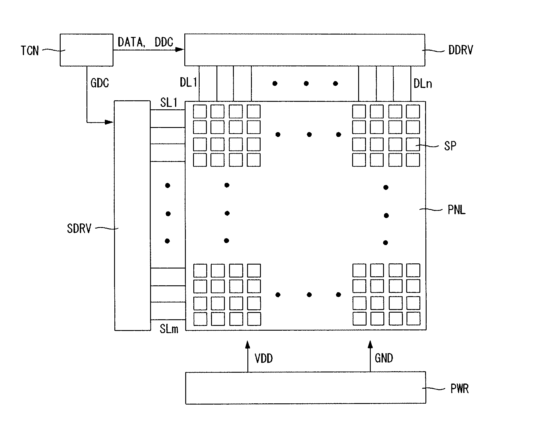
Organic light emitting diode display
a technology of light-emitting diodes and display panels, which is applied in the field of organic light-emitting diodes (oled) display panels, can solve problems such as the increase of the bezel area
- Summary
- Abstract
- Description
- Claims
- Application Information
AI Technical Summary
Problems solved by technology
Method used
Image

Examples
first exemplary embodiment
[0032]FIG. 3 is a plane view illustrating a structure of an OLED display according to a first exemplary embodiment of the invention. FIG. 4 is a cross-sectional view of an area A1-A2 of FIG. 3. FIG. 5 is a cross-sectional view of an area B1-B2 of FIG. 3.
[0033]As shown in FIG. 3, a substrate constituting the panel PNL includes a display area AA and non-display areas BZx1, BZx2, BZy1, and BZy2. The non-display areas BZx1, BZx2, BZy1, and BZy2 include a first non-display area BZx1 corresponding to a first side, a second non-display area BZx2 corresponding to a second side, a third non-display area BZy1 corresponding to a third side, and a fourth non-display area BZy2 corresponding to a fourth side. The display area AA is defined as a display unit DSP by the subpixels SP arranged in the matrix form. The non-display areas BZx1, BZx2, BZy1, and BZy2 are defined as a bezel area BZA by a main ground line MGND and an auxiliary ground line AGND. The main ground line MGND and the auxiliary gro...
second exemplary embodiment
[0041]FIG. 6 is a plane view illustrating a structure of an OLED display according to a second exemplary embodiment of the invention.
[0042]As shown in FIG. 6, the OLED display according to the second exemplary embodiment of the invention is substantially the same as the OLED display according to the first exemplary embodiment, except that first and second main ground lines MGND1 and MGND2 are respectively formed in first and second non-display areas BZx1 and BZx2.
[0043]Hence, the first main ground line MGND1 and an auxiliary ground line AGND partially overlap each other in the first non-display area BZx1 and are electrically connected to each other. Further, the second main ground line MGND2 and the auxiliary ground line AGND partially overlap each other in the second non-display area BZx2 and are electrically connected to each other.
third exemplary embodiment
[0044]FIG. 7 is a plane view illustrating a structure of an OLED display according to a third exemplary embodiment of the invention. FIG. 8 is a cross-sectional view of an area C1-C2 of FIG. 7.
[0045]As shown in FIG. 7, a substrate constituting the panel PNL includes a display area AA and non-display areas BZx1, BZx2, BZy1, and BZy2. The non-display areas BZx1, BZx2, BZy1, and BZy2 include a first non-display area BZx1 corresponding to a first side, a second non-display area BZx2 corresponding to a second side, a third non-display area BZy1 corresponding to a third side, and a fourth non-display area BZy2 corresponding to a fourth side. The display area AA is defined as a display unit DSP by the subpixels SP arranged in the matrix form. The non-display areas BZx1, BZx2, BZy1, and BZy2 are defined as a bezel area BZA by a main ground line MGND and an auxiliary ground line AGND. The main ground line MGND and the auxiliary ground line AGND on the panel PNL are connected to a ground line...
PUM
 Abstract
Description
Claims
Application Information