

Loop antenna
a technology of loop antenna and loop antenna, which is applied in the direction of antennas, electrically long antennas, electrical equipment, etc., can solve the problem of not being able to obtain satisfactory characteristics
- Summary
- Abstract
- Description
- Claims
- Application Information
AI Technical Summary
Benefits of technology
Problems solved by technology
Method used
Image

Examples
first embodiment
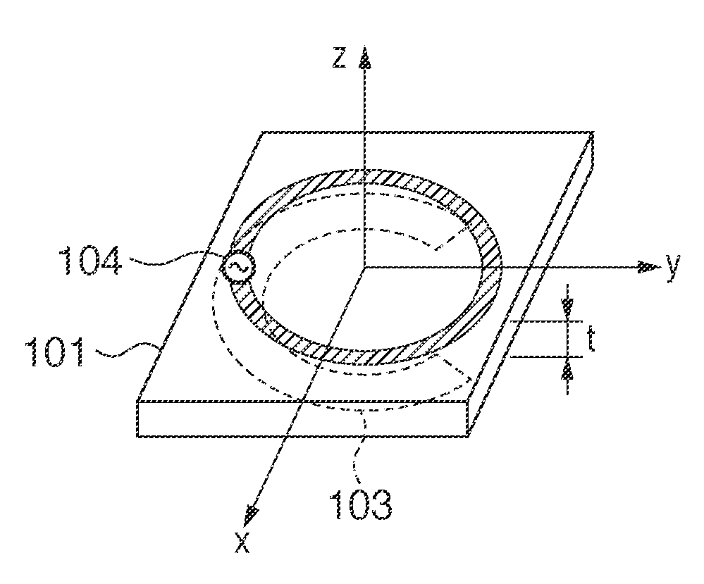
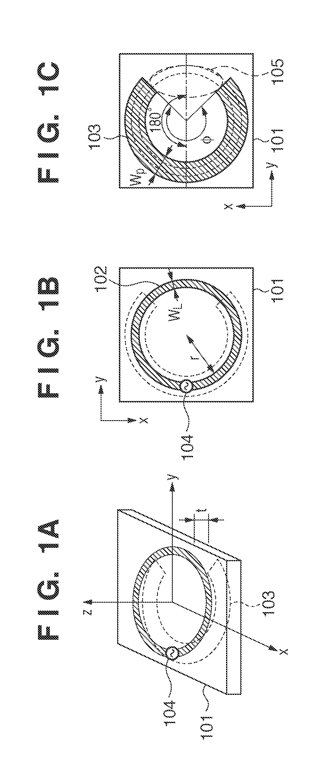
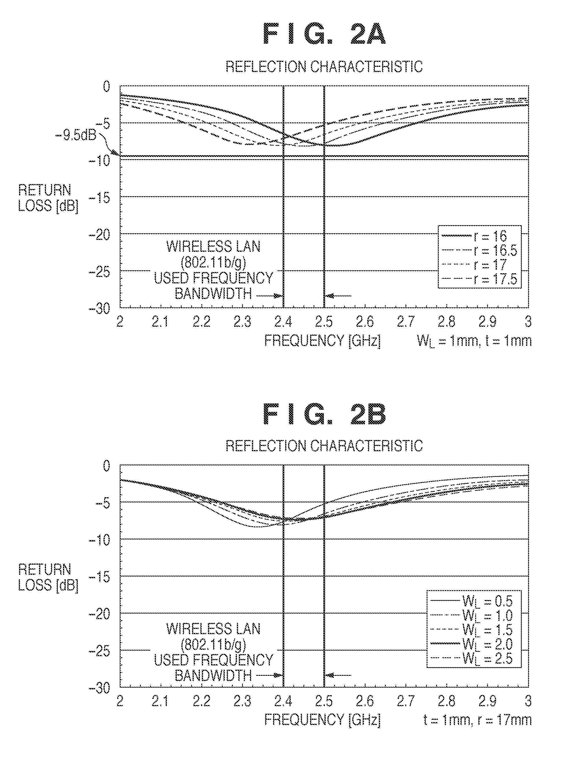
[0033]The arrangement of a loop antenna according to the first embodiment will be described with reference to FIGS. 1A to 1C. A circular loop element (to be simply referred to as a loop element hereinafter) 102 of a conductor is arranged (FIG. 1B) on one surface (upper surface) of a dielectric substrate 101 (FIG. 1A). A circular parasitic element (to be simply referred to as a parasitic element hereinafter) 103 of a conductor is arranged (FIG. 1C) on the other surface (lower surface) on the other side of the one surface. The parasitic element 103 and the loop element 102 are arranged such that the line connecting the center point of the parasitic element 103 on the x-y plane and that of the loop element 102 on the x-y plane guarantees an almost concentric relationship and is perpendicular to the surfaces of the dielectric substrate 101. Note that the line connecting the center point of the parasitic element 103 on the x-y plane and that of the loop element 102 on the x-y plane can g...
second embodiment
[0049]In this embodiment, an example will be explained in which Teflon™ is used as a different dielectric material. The arrangement of the loop antenna is the same as in FIGS. 1A to 1C of the first embodiment. Teflon is a material having a dielectric constant smaller than that of glass epoxy used for the dielectric substrate 101 of the first embodiment, and its relative dielectric constant to be used for calculation is assumed to be 2.1 in the simulations. The frequency bandwidth used in wireless communication is 2.4 to 2.5 GHz, as in the first embodiment. The design is done by the same parameter setting method as described in the first embodiment. When the thickness of a dielectric substrate 101 is t=1 mm, the loop radius of a loop element 102 is r=18.5 mm. The loop radius is larger for Teflon than for glass epoxy because the dielectric constant of Teflon is smaller than that of glass epoxy. At this time, the loop width is WL=1 mm, and the width of the parasitic element is Wp=3 mm....
third embodiment
[0050]In this embodiment, an example will be explained in which a frequency different from that of the first embodiment is used as the frequency bandwidth used in wireless communication. In this embodiment, as the frequency bandwidth used in wireless communication, the frequency bandwidths of IEEE802.11a, that is, 5.15 to 5.35 GHz and 5.47 to 5.725 GHz will be described as examples of the desired frequency bandwidth. The arrangement of the loop antenna is the same as in FIGS. 1A to 1C of the first embodiment. A dielectric substrate 101 is made of glass epoxy, as in the first embodiment. The parameters of the loop antenna are designed by the same setting method as described in the first embodiment. When the thickness of the dielectric substrate 101 is t=1 mm, the radius of a loop element 102 is r=7.5 mm. At this time, the center frequency of the frequency bandwidth used in wireless communication is about 5.5 GHz. Hence, the radius of the loop element 102, which causes the loop antenn...
PUM
 Abstract
Description
Claims
Application Information