Liquid Crystal Display Device

a display device and liquid crystal technology, applied in non-linear optics, instruments, optics, etc., can solve the problems of difficult electric field formation and increase in manufacturing costs, and achieve the effects of reducing manufacturing costs, wide viewing angle characteristics, and improving transmittan

Active Publication Date: 2012-03-22
JAPAN DISPLAY CENTRAL CO LTD
View PDF6 Cites 2 Cited by
  • Summary
  • Abstract
  • Description
  • Claims
  • Application Information

AI Technical Summary

Benefits of technology

[0009]The present invention has been made in consideration of the above-described problems, and the object of the invention is to provide a liquid crystal display device which suppresses the manufacturing cost, has wide viewing angle characteristics, improves the transmittance, and has good display quality.
[0011]The present invention can provide a liquid crystal display device which suppresses the manufacturing cost, has wide viewing angle characteristics, improves the transmittance, and has good display quality.

Problems solved by technology

This may cause an increase in manufacturing cost.
Furthermore, in the transverse-electric-field-mode liquid crystal display device, it is difficult to form an electric field, which is parallel to the major surface of the substrate, over the pixel electrode.

Method used


Image

  • Liquid Crystal Display Device
  • Liquid Crystal Display Device
  • Liquid Crystal Display Device

Examples


Embodiment Construction

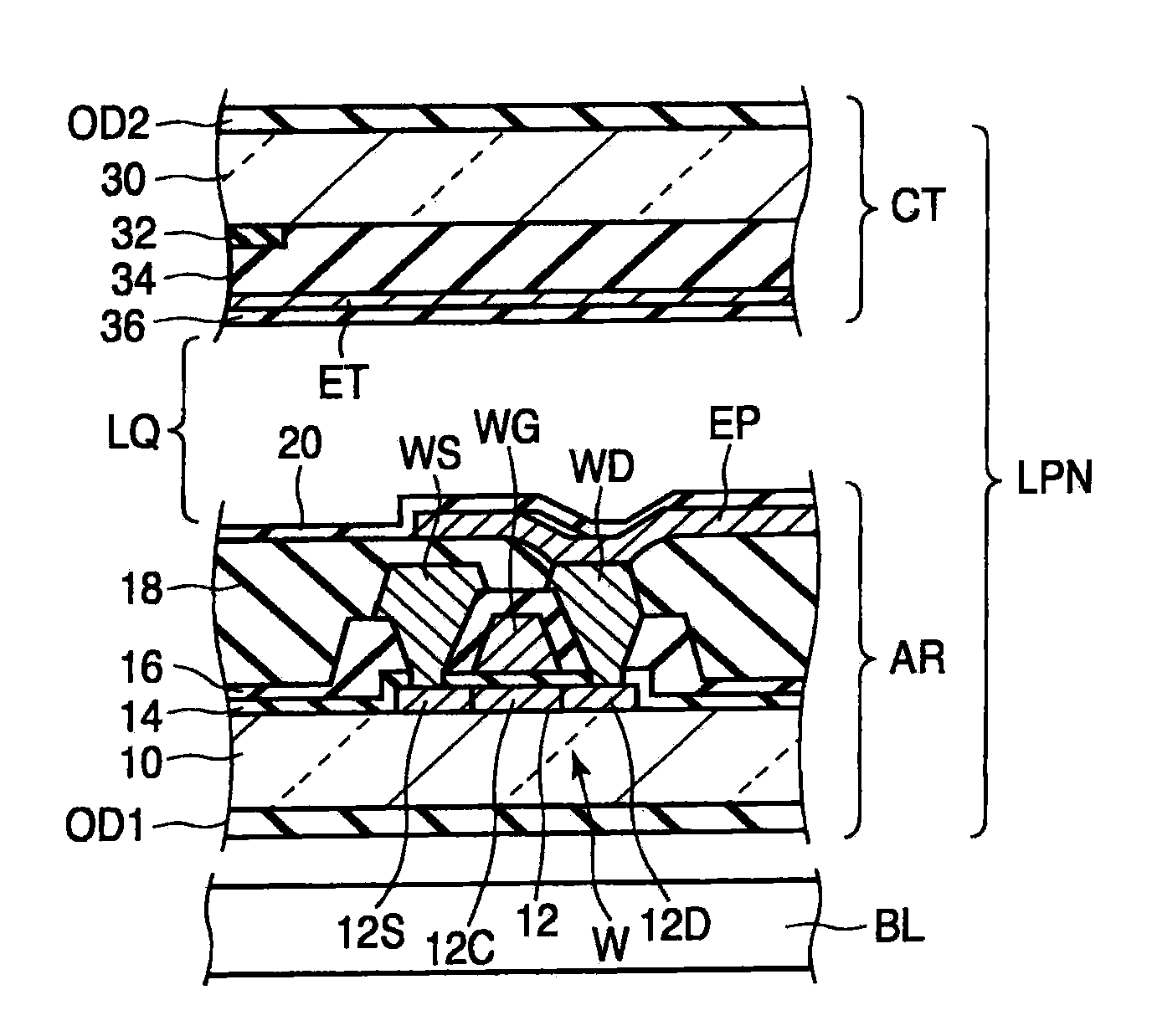
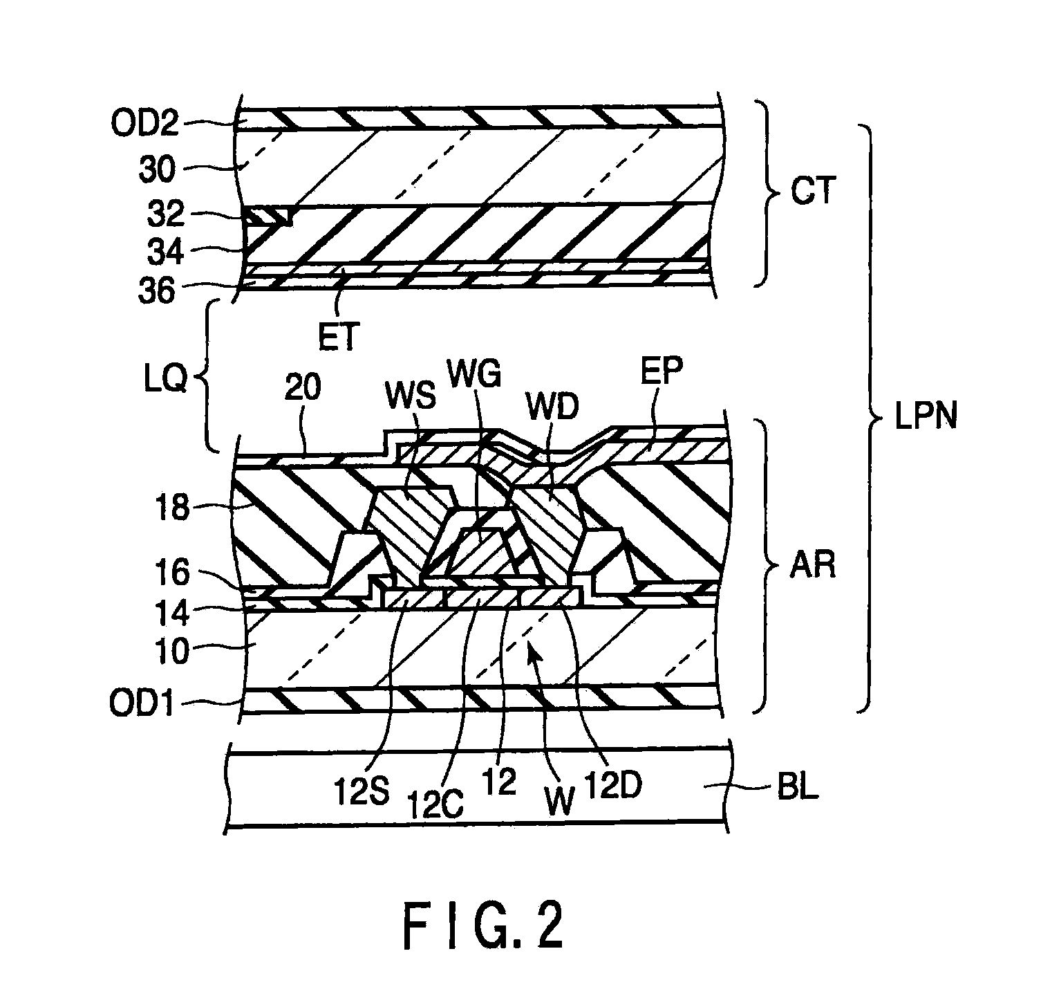
[0027]A liquid crystal display device according to an embodiment of the present invention will now be described with reference to the accompanying drawings. In the description below, exemplification is made of a liquid crystal mode in which an array substrate includes a pixel electrode, a counter-substrate includes a counter-electrode, and liquid crystal molecules are switched by mainly using a transverse electric field which is formed between the pixel electrode and the counter-electrode (i.e. an electric field which is substantially parallel to the major surface of the array substrate).

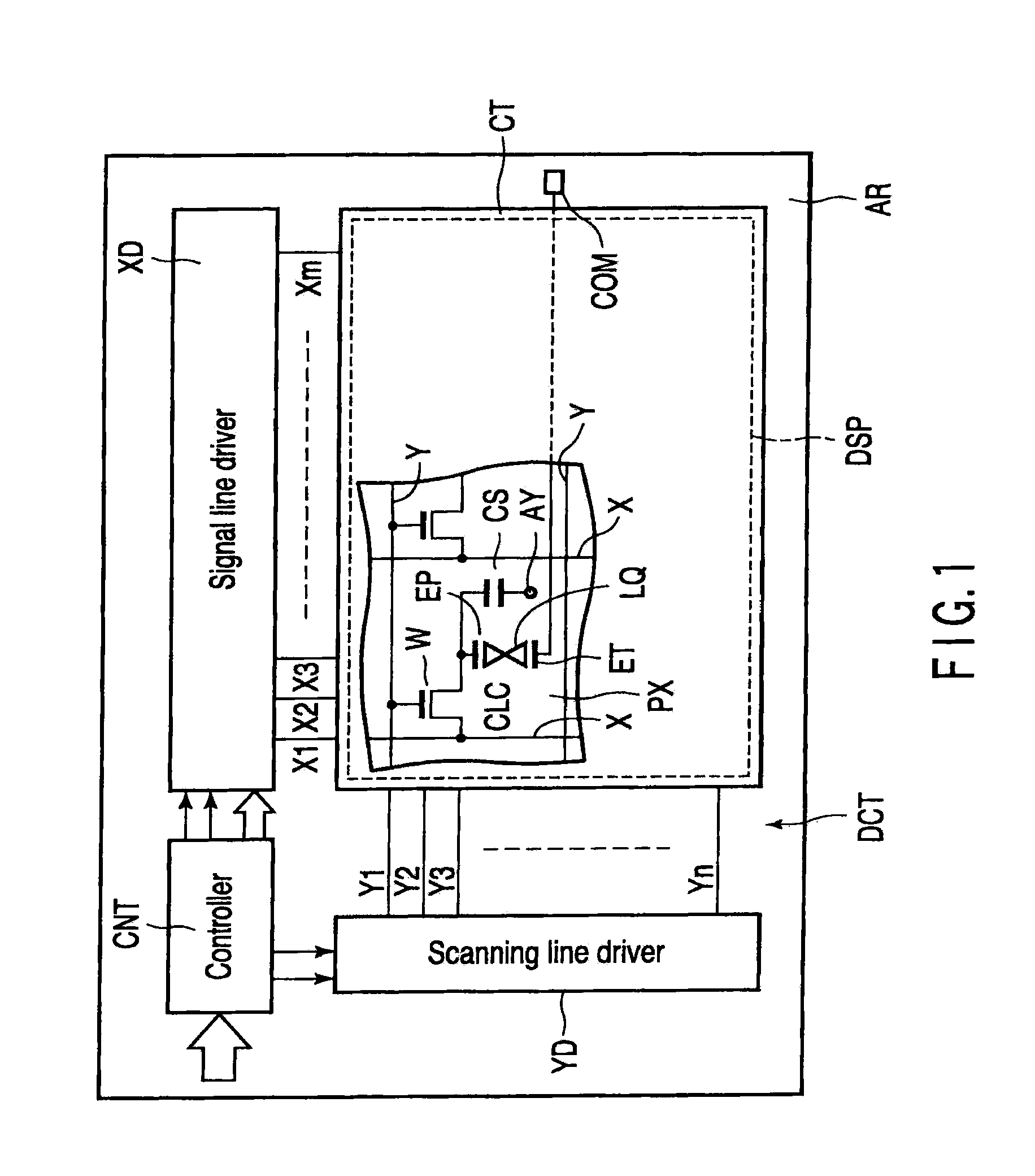
[0028]As shown in FIG. 1, FIG. 2 and FIG. 3, the liquid crystal display device is an active matrix liquid crystal display device, and includes a liquid crystal display panel LPN. The liquid crystal display panel LPN includes a pair of substrates, namely, an array substrate AR and a counter-substrate CT which is disposed to be opposed to the array substrate AR.

[0029]Further, the liquid crystal displa...


PUM

PropertyMeasurementUnit
transmittanceaaaaaaaaaa
storage capacitanceaaaaaaaaaa

Abstract

A liquid crystal display device includes an array substrate including a pixel electrode which is disposed in each of pixels, a counter-substrate which is disposed to be opposed to the array substrate and includes a counter-electrode which is common to a plurality of the pixels, and a liquid crystal layer which is held between the array substrate and the counter-substrate. The pixel electrode includes a first major electrode portion having a strip shape, and the counter-electrode includes second major electrode portions each having a strip shape, the second major electrode portions being disposed in parallel to the first major electrode portion in a manner that the first major electrode portion is interposed between the second major electrode portions and that the first major electrode portion and the second major electrode portions are alternately arranged.

Description

CROSS-REFERENCE TO RELATED APPLICATIONS[0001]This application is based upon and claims the benefit of priority from prior Japanese Patent Application No. 2008-033437, filed Feb. 14, 2008, the entire contents of which are incorporated herein by reference.BACKGROUND OF THE INVENTION[0002]1. Field of the Invention[0003]The present invention relates generally to a liquid crystal display device, and more particularly to a liquid crystal display device which includes a pixel electrode on an array substrate, includes a counter-electrode on a counter-substrate, and generates a transverse electric field between the pixel electrode and the counter-electrode.[0004]2. Description of the Related Art[0005]In recent years, flat-panel display devices have vigorously been developed, and liquid crystal display devices attract particular attention by virtue of their advantages of light weight, small thickness and low power consumption. In particular, in an active matrix liquid crystal display device i...

Claims


Application Information

Patent Timeline
Patent Type & Authority Applications(United States)
IPC IPC(8): G02F1/1337G02F1/1343
CPCG02F1/133784G02F1/134363
Inventor HIROSAWA, JIN
Owner JAPAN DISPLAY CENTRAL CO LTD
Why Eureka
Try Eureka