

Liquid crystal panel, method for manufacturing same, and liquid crystal display device
- Summary
- Abstract
- Description
- Claims
- Application Information
AI Technical Summary
Benefits of technology
Problems solved by technology
Method used
Image

Examples
example 1
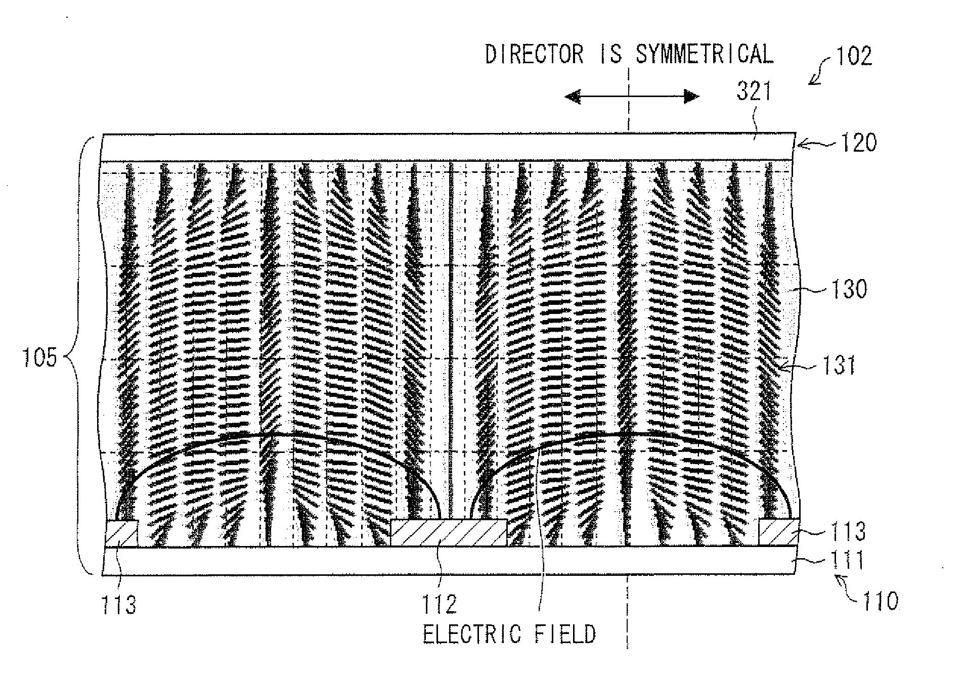
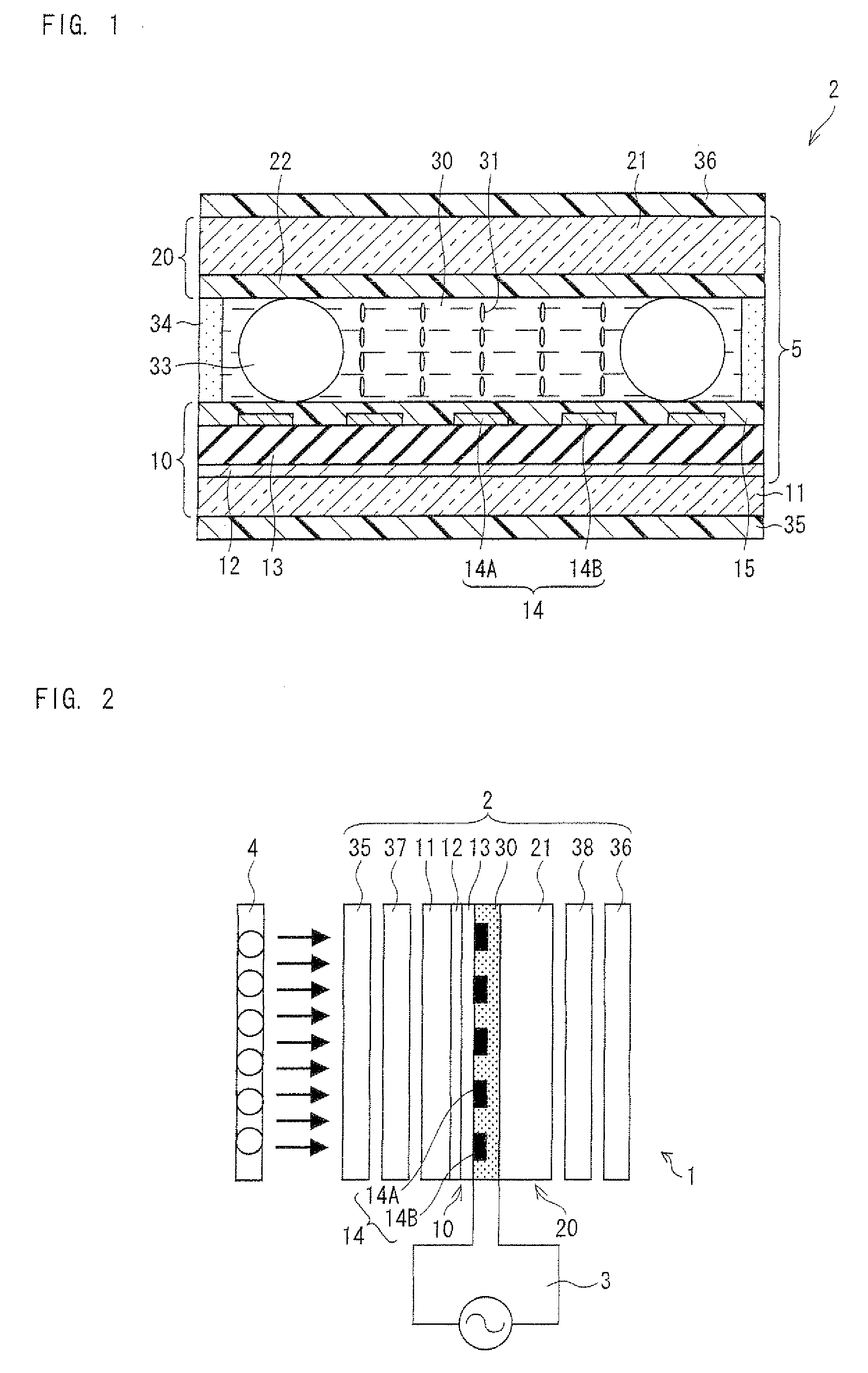
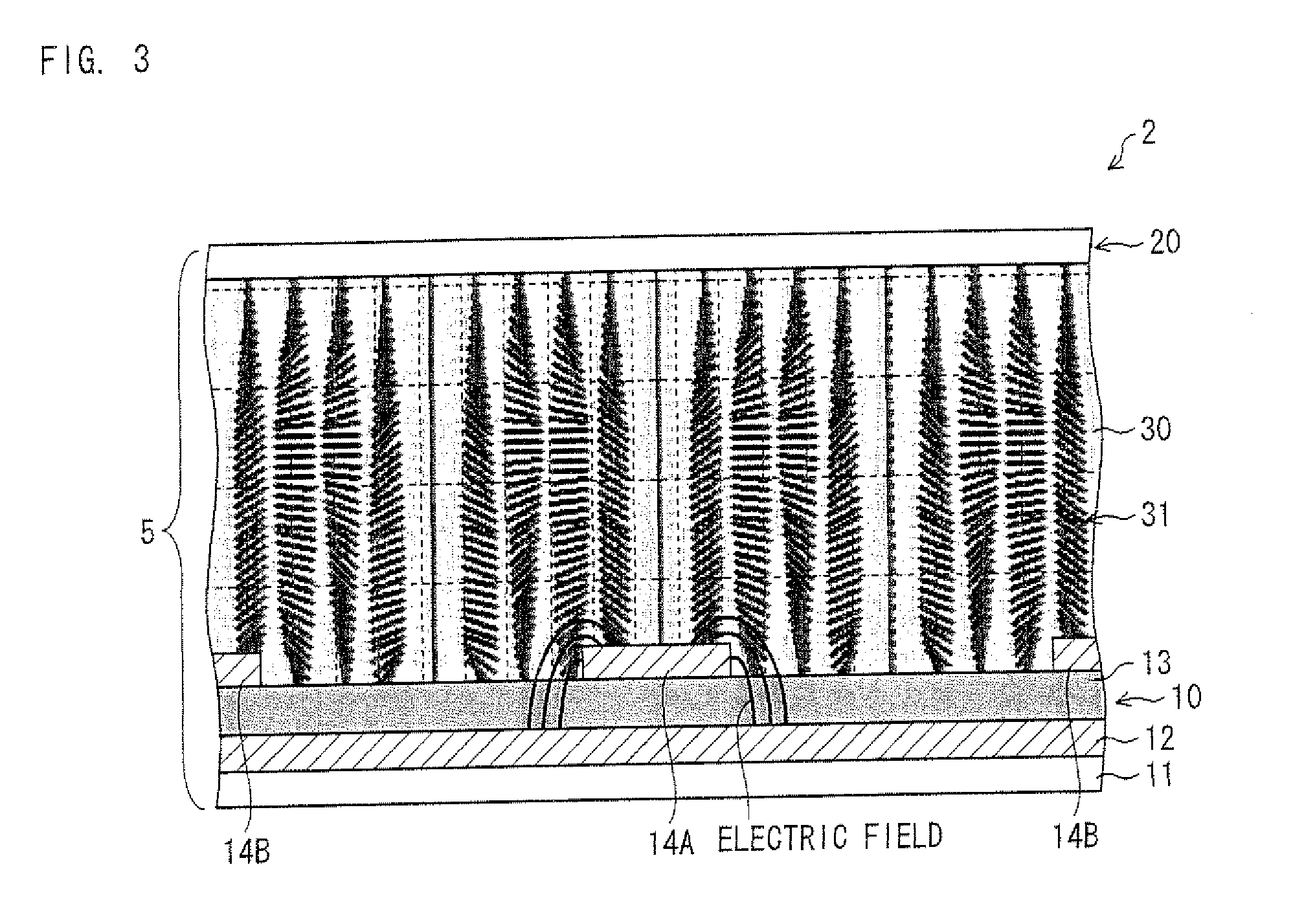
[0125]First, ITO (Indium Tin Oxide) was formed on an entire surface of a glass substrate 11 by sputtering so as to have a thickness of 1400 Å, as shown in FIG. 1. Thus, a lower electrode 12 which is an allover electrode which covers an entire main surface of the glass substrate 11 was formed.
[0126]Next, silicon nitride (SiN) having a relative permittivity ∈ of 6.9 was formed by sputtering so as to cover an entire surface of the lower electrode 12. Thus, an insulating layer 13 made of SiN having a thickness d of 0.1 μm (1000 Å) was formed on the lower electrode 12.
[0127]Subsequently, comb electrodes 14A and 14B which were made of ITO and which had an thickness of 1400 Å, an electrode width L of 2.6 μm, and an electrode spacing S of 8.0 μm was formed, as an upper electrode, on the insulating layer 13.
[0128]Then, an alignment film material “JALS-204” (Product Name, 5% by weight (solid content), γ-butyrolactone solution, produced by JSR Corporation) was applied, by a spin coat method, o...
example 2
[0137]Actual measurement T and SimT were obtained in a similar manner to the Example 1 except for that FFS driving was carried out instead of comb driving.
[0138]That is, in the present example, a liquid crystal panel 2 similar to that of the Example 1 was fabricated by using a material and a process similar to the Example 1, and the measurement T was measured on the backlight 4 by using the “BM5A” as in the Example 1. Moreover, SimT obtained in a case where a model having an FFS structure similar to that of the Example 1 was FFS-driven under the same condition as the actual measurement was measured by running a simulation with the use of the “LCD-MASTER” as in the Example 1.
[0139]Table 1 collectively shows the SimT, relative permittivity ∈ and thickness d of the insulating layer 13, and electrode width L / electrode spacing S of the comb electrodes 14A and 14B. Table S shows the actual measurement T and the electrical energy EL in addition to these values. (a) of FIG. 5 shows an appli...
example 3
[0163]SimT was obtained in a similar manner to the Example 2 except for that the thickness of the insulating layer 13 was changed from 0.1 μm to 0.3 μm (3000 Å).
[0164]Table 1 collectively shows the SimT, relative permittivity ∈ and thickness d of the insulating layer 13, and electrode width L / electrode spacing S of the comb electrodes 14A and 14B. Table 8 shows the electrical energy EL in addition to these values. (a) of FIG. 6 shows an applied voltage in the simulation, and (b) of FIG. 6 shows transmittance, a director distribution of the liquid crystal molecules 31, and an equipotential curve achieved when a voltage of 6V is applied to each of the comb electrodes 14A and 14B in (a) of FIG. 6 in the simulation, (c) of FIG. 6 shows how a pixel is displayed in a case where power is off in the simulation and how a pixel is displayed in a case where power is on in the simulation.
PUM
 Abstract
Description
Claims
Application Information