This helps you quickly interpret patents by identifying the three key elements:
Problems solved by technology
Method used
Benefits of technology
Benefits of technology
[0013]It is therefore an object of the present invention to provide a producing method of a wired circuit board which allows an inspection of a conductive pattern and an inspection of a foreign matter present on an insulating base layer exposed from the conductive pattern to be performed easily and simultaneously.
[0019]This allows each of the contrast between the pattern reflected light and the table reflected light and the contrast between the table reflected light and the foreign-matter reflected light to be set high in a well-balanced manner.
[0020]Therefore, it is possible to easily and simultaneously perform an inspection of the conductive pattern and an inspection of the foreign matter present on the insulating base layer exposed from the conductive pattern.
Problems solved by technology
As a result, it is difficult to inspect the foreign matter 46 present on the upper surface of the insulating base layer 42 exposed from the conductive pattern 41.
Method used
Image
Click on the blue label to locate the original text in one second.
Reading with bidirectional positioning of images and text.
Examples
example 1
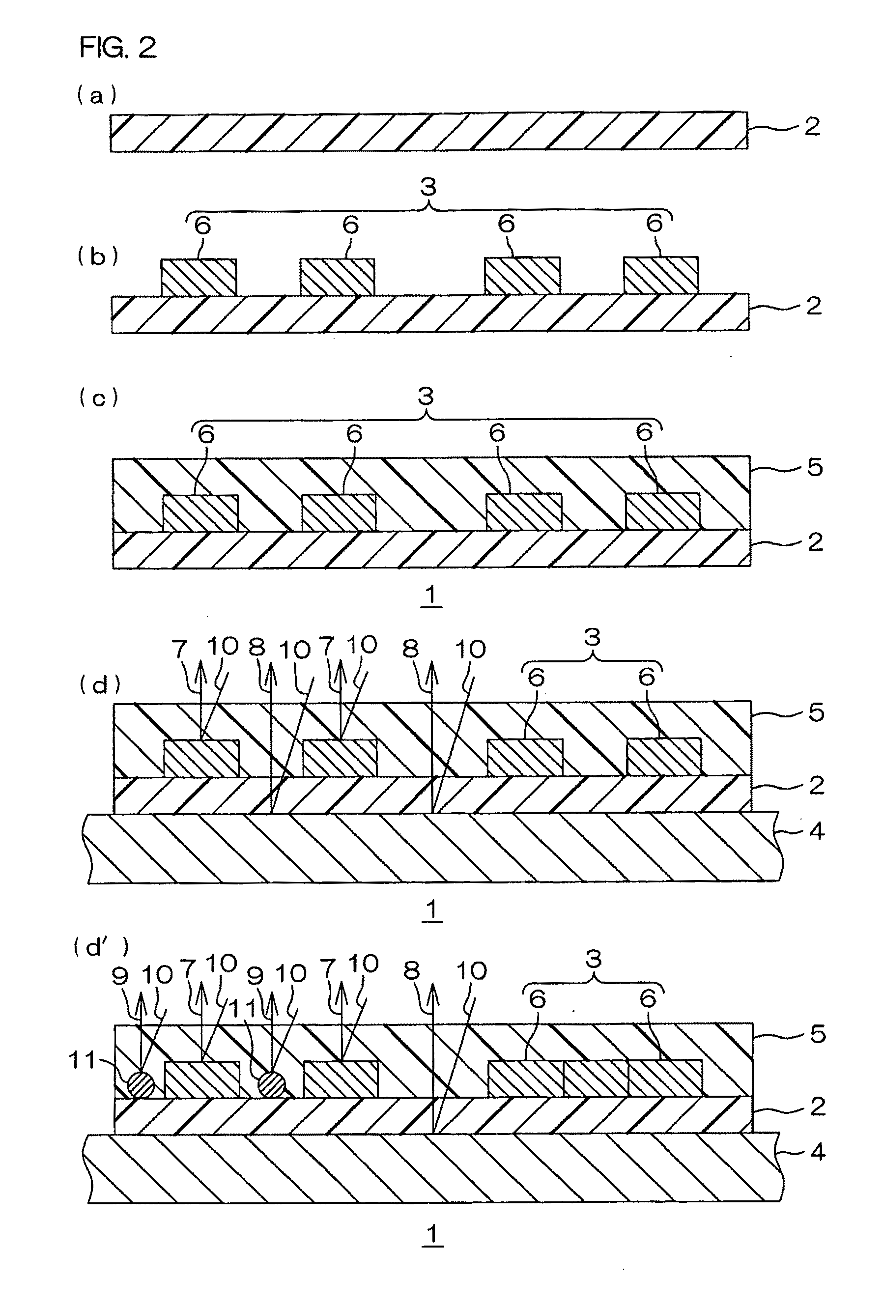
[0114]By a roll-to-roll method using the conveying device shown in FIG. 3 described above, the following steps were performed in succession to produce a flexible wired circuit board.
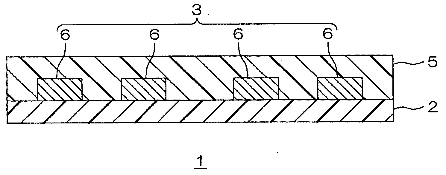
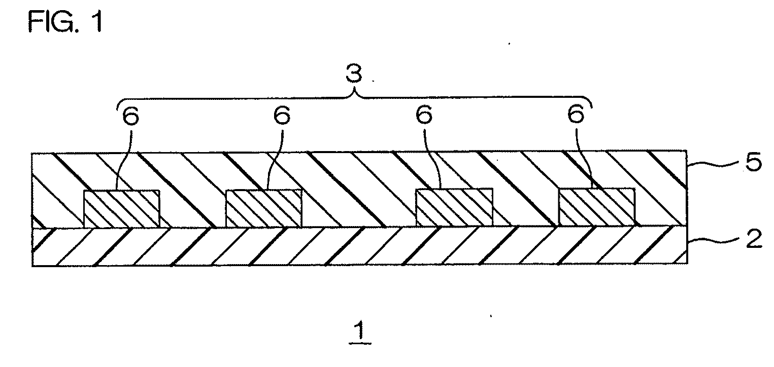
[0115]That is, an insulating base layer made of polyimide (A) and in the shape of an elongated sheet having a width of 300 mm and a thickness of 12.5 μm was prepared (see FIG. 2(a)).
[0116]Then, on the insulating base layer, a conductive pattern made of copper and having a thickness of 8 μm was formed in a wired circuit pattern having wires and terminal portions by an additive method (see FIG. 2(b)). The width of each of the wires was 30 μm. The width of each of the terminal portions was 30 μm. The spacing between the individual wires was 60 μm. The widthwise spacing between the individual terminal portions was 60 μm.
[0117]Then, carbon black (foreign matter) having an average particle diameter of 20 μm was mixed onto the insulating base layer exposed from the wires.
[0125]An inspection step was performed in the same manner as in EXAMPLE 1 except that an inspection device including a support table having a surface thereof formed with a copper film having a thickness of 0.5 μm instead of the tin film was used in the inspection step.
[0126]An image processed view obtained by data processing is shown in FIG. 7, and evaluation in the inspection is shown in Table 1.
example 3
[0127]A flexible wired circuit board was prepared in the same manner as in EXAMPLE 1 except that, in the preparation of the flexible wired circuit board, the material and thickness of the insulating base layer were changed to polyimide (B) and 18 μm, and the material and thickness of the insulating cover layer were changed to the polyimide (B) and 18 μm.
[0128]Then, the inspection step was performed in the same manner as in EXAMPLE 1 except that, in the inspection step, an inspection device including a support table having a surface thereof formed with a copper film having a thickness of 0.5 μm instead of the tin film was used, and light at a wavelength of 720 nm was used instead of the light at a wavelength of 670 nm.
[0129]An image processed view obtained by data processing is shown in FIG. 8, and evaluation in the inspection is shown in Table 1.
[0130]Separately from the flexible wired circuit board, sheets each made of the polyimide (B), which was the same material as those of the ...
PUM
Property
Measurement
Unit
Fraction
aaaaa
aaaaa
Fraction
aaaaa
aaaaa
Wavelength
aaaaa
aaaaa
Abstract
A producing method of a wired circuit board includes the steps of preparing the wired circuit board, placing the wired circuit board on a support table, and applying light from above the wired circuit board toward the wired circuit board, and sensing pattern reflected light, table reflected light and foreign-matter reflected light to inspect the conductive pattern and the foreign matter based on a contrast therebetween. In the step of inspecting the conductive pattern and the foreign matter, a reflectance of the table reflected light is in a range of 25 to 55%, and a reflectance of the foreign-matter reflected light is in a range of not more than 10%.
Description
CROSS-REFERENCE TO RELATED APPLICATIONS[0001]This patent application priority from Japanese Patent Application No. 2009-099198, filed on Apr. 15, 2009, the contents of which are herein incorporated by reference in their entirety.BACKGROUND OF THE INVENTION[0002]1. Field of the Invention[0003]The present invention relates to a producing method of a wired circuit board and, more particularly, to a producing method of a wired circuit board such as a flexible wired circuit board.[0004]2. Description of the Related Art[0005]A wired circuit board such as a flexible wired circuit board has an insulating base layer, a conductive pattern formed thereon, and an insulating cover layer formed on the insulating base layer so as to cover the conductive pattern. It has been known that, in the production of such a wired circuit board, an insulating base layer, a conductive pattern, and an insulating cover layer are successively formed, and then the shape of the conductive pattern is optically inspe...
Claims
Application Information
Patent Timeline
Application Date:The date an application was filed.
Publication Date:The date a patent or application was officially published.
First Publication Date:The earliest publication date of a patent with the same application number.
Issue Date:Publication date of the patent grant document.
PCT Entry Date:The Entry date of PCT National Phase.
Estimated Expiry Date:The statutory expiry date of a patent right according to the Patent Law, and it is the longest term of protection that the patent right can achieve without the termination of the patent right due to other reasons(Term extension factor has been taken into account ).
Invalid Date:Actual expiry date is based on effective date or publication date of legal transaction data of invalid patent.

