Method of manufacturing light emitting diode package

Inactive Publication Date: 2012-03-29
ADVANCED OPTOELECTRONICS TECH
View PDF4 Cites 14 Cited by
  • Summary
  • Abstract
  • Description
  • Claims
  • Application Information

AI Technical Summary

Problems solved by technology

During the insert molding of the encapsulating material, the encapsulating material is prone to spill over the reflecting cup, and unevenly cover the

Method used


Image

  • Method of manufacturing light emitting diode package
  • Method of manufacturing light emitting diode package
  • Method of manufacturing light emitting diode package

Examples


Example

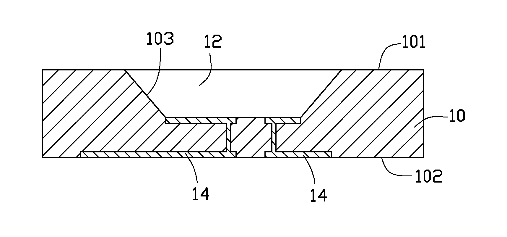
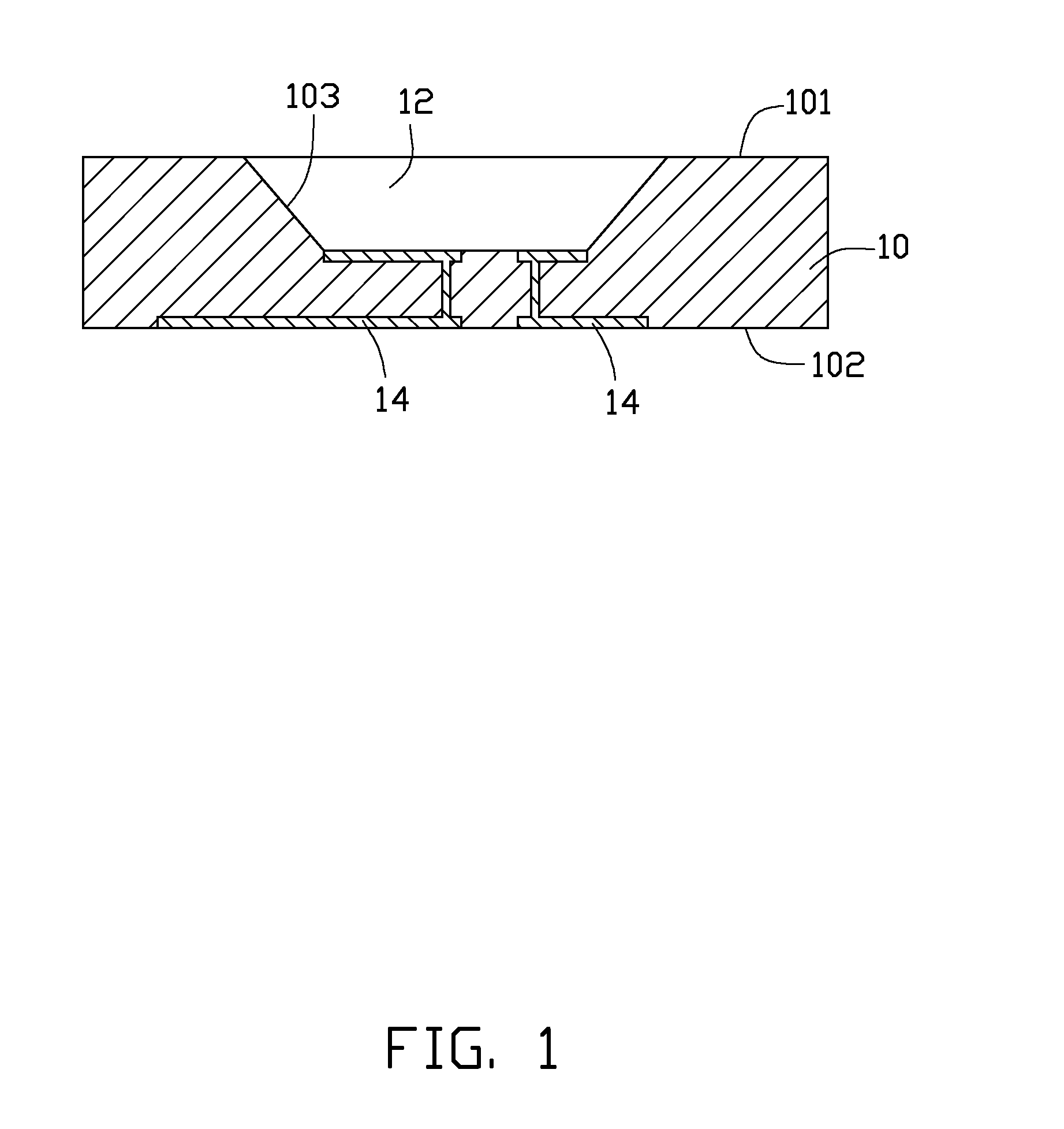
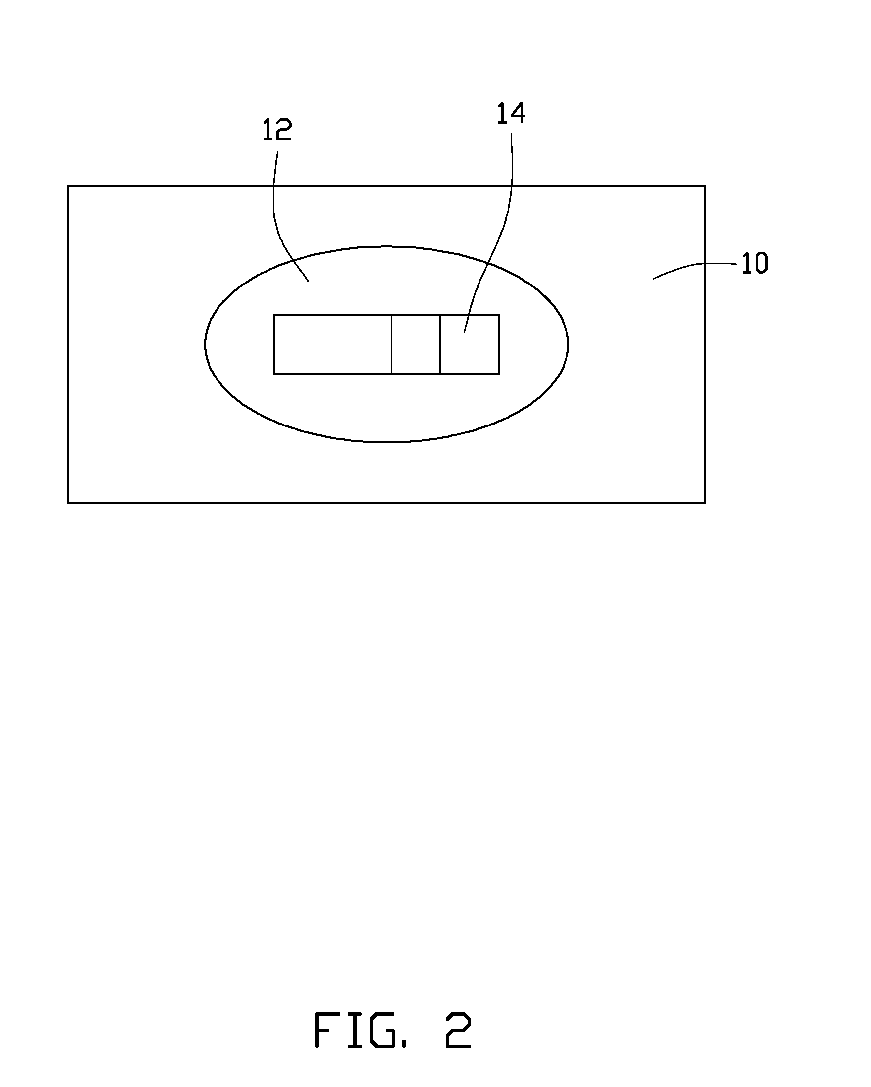
[0011]A method of manufacturing an LED package provided by the present disclosure substantially comprises bonding, encapsulating and baking. Firstly, a base 10 is provided. FIG. 1 is a cross sectional view of the base 10, and FIG. 2 is a top view of the base 10. The base 10 comprises a first surface 101 and an opposite second surface 102. The first surface 101 may be a top surface, and the second surface 102 may be a bottom surface. A receiving recess 12 is defined in the first surface 101. An inner surface 103 of the base 10 surrounding the receiving recess 12 functions as a reflecting cup. Referring to FIG. 2, the receiving recess 12 has a substantially elliptic top opening. A bottom of the receiving recess 12 has a rectangular shape, and is substantially parallel to the first surface 101. A width of the receiving recess 12 increases gradually along a bottom-to-top direction, meanwhile a depth of the receiving recess 12 increases along a periphery-to-center direction. The depth of...


PUM

PropertyMeasurementUnit
Pressureaaaaaaaaaa
Speedaaaaaaaaaa
Depthaaaaaaaaaa

Abstract

An exemplary method of manufacturing an LED package includes providing a base, the base having a reflecting cup with a receiving recess defined therein; an LED chip is then mounted on the base and secured in a bottom of the receiving recess; thereafter, a dispensing nozzle is used to apply an encapsulating material into the receiving recess to encapsulate the LED chip; finally, the encapsulating material is baked to form an encapsulating layer. The dispensing nozzle moves relative to the receiving recess during the application of the encapsulating material. A depth of the receiving recess is varied. Parameters of the application of the encapsulating material into the receiving recess by the dispensing nozzle vary in response to a change of the depth of the receiving recess.

Description

BACKGROUND[0001]1. Technical Field[0002]The present disclosure relates generally to light emitting devices, and more particularly to a method of manufacturing a light emitting diode (LED) package.[0003]2. Description of Related Art[0004]LEDs are solid state light emitting devices formed of semiconductors, which are more stable and reliable than other conventional light sources such as incandescent bulbs. Thus, LEDs are being widely used in various fields such as numeral / character displaying elements, signal lights, light sources for lighting and display devices. When in use, providing LEDs in packages can provide protection, color selection, focusing and the like for light emitted by the LEDs. Generally, a process of packaging an LED chip includes bonding, encapsulating, baking, cutting etc.[0005]In a typical packaging process, an encapsulating material such as a viscous, jelly-like material is brought to fill into a reflecting cup in which the LED chip is mounted to cover the LED c...

Claims


Application Information

Patent Timeline
IPC IPC(8): H01L33/52H01L33/60
CPCB29C31/045B29C39/10H01L2933/005H01L33/60H01L33/52H01L2224/16225H01L2924/181H01L2924/00012
Inventor CHANG, CHAO-HSIUNGHU, PI-CHIANG
Owner ADVANCED OPTOELECTRONICS TECH
Why Eureka
Try Eureka