Light emitting diode package and light emitting diode module

a technology of light-emitting diodes and led modules, which is applied in the direction of basic electric elements, electrical equipment, and semiconductor devices, etc., can solve the problems of affecting the soldering the led package floats or inclination, and the solder paste is prone to spill over the base of the led package,

Inactive Publication Date: 2012-02-02
ADVANCED OPTOELECTRONICS TECH
View PDF3 Cites 5 Cited by
  • Summary
  • Abstract
  • Description
  • Claims
  • Application Information

AI Technical Summary

Benefits of technology

[0005]A typical LED package includes a base with an LED chip encapsulated thereon. The LED package is generally formed as a surface mounting type device for facilitating application, whereby the base is mounted on a printed circuit board or other similar elements. Solder paste such as tin is used between the base and the printed circuit board for soldering the LED package on the printed circuit board. However, the existent of solder paste easily results in floating or inclination of the LED package. When heating the solder paste to bond the LED package onto the printed circuit board, the solder paste is prone to spill over the base of the LED package. The above mentioned factors not only interfere the soldering of the LED package, but also destroy aesthetics of the LED package. In addition, the solder paste is also prone to generate voids therein due to heating flux thereof, which increases a heat resistance of the solder paste and negatively affects the heat dissipation of the LED package.

Problems solved by technology

However, the existent of solder paste easily results in floating or inclination of the LED package.
When heating the solder paste to bond the LED package onto the printed circuit board, the solder paste is prone to spill over the base of the LED package.
The above mentioned factors not only interfere the soldering of the LED package, but also destroy aesthetics of the LED package.
In addition, the solder paste is also prone to generate voids therein due to heating flux thereof, which increases a heat resistance of the solder paste and negatively affects the heat dissipation of the LED package.

Method used


Image

  • Light emitting diode package and light emitting diode module
  • Light emitting diode package and light emitting diode module
  • Light emitting diode package and light emitting diode module

Examples


third embodiment

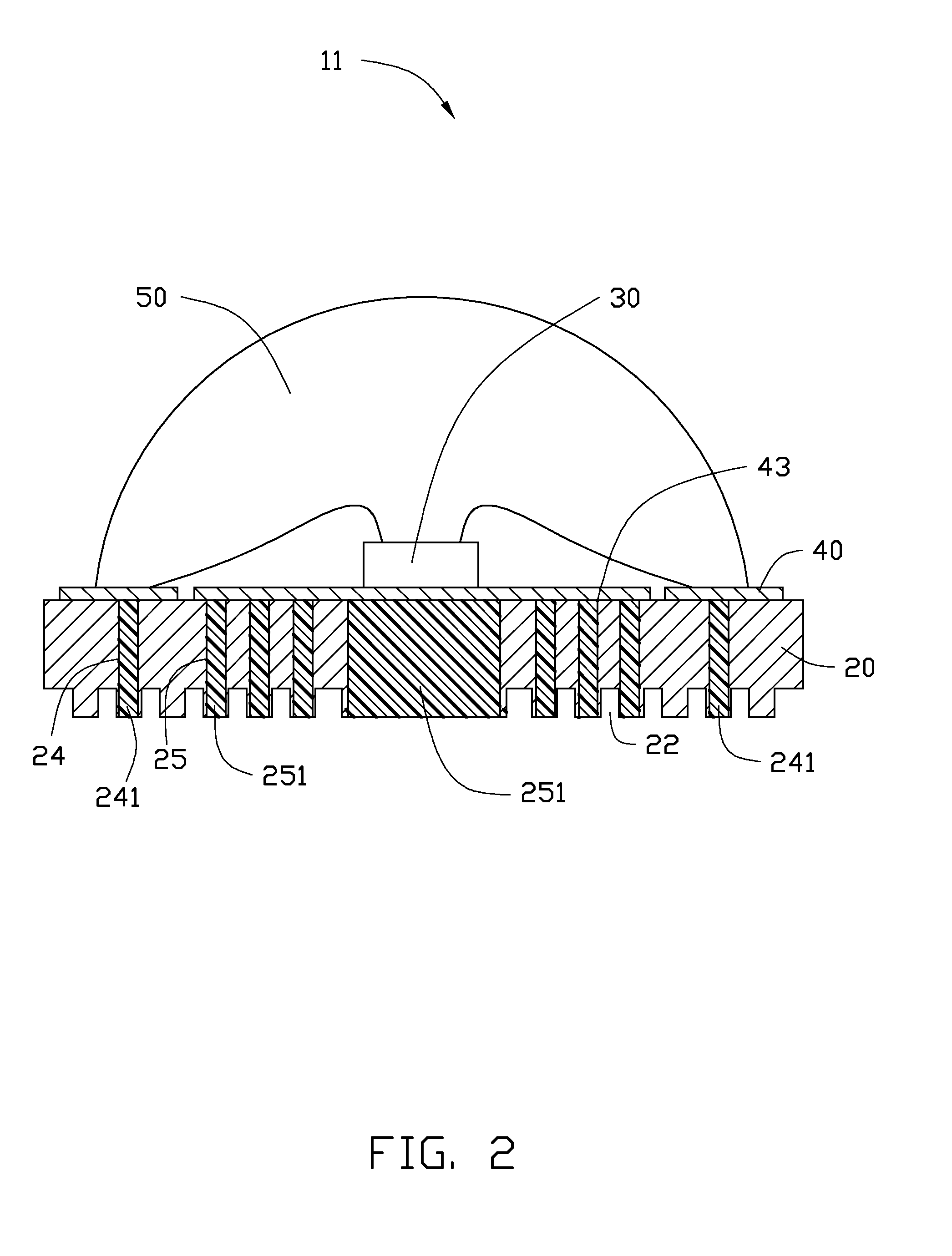
[0025]The grooves22 are defined in the base 20 by machining the base 20 in the previous embodiments. It is understood that the grooves 22 can also be defined by other fashions. Referring to FIG. 3, the base 20 in a third embodiment comprises a plurality of plate-shaped electrically conductive materials 241 and heat conductive materials 251 (such as metal), and a plurality of plate-shaped, electrically isolating materials 201 (such as ceramics, plastic, etc.) presented in an alternating fashion. The electrically conductive materials 241 and heat conductive materials 251, and the isolating materials 201 are vertically placed. The electrically conductive materials 241 and heat conductive materials 251 are higher than the isolating materials 201. Tops of the electrically conductive materials 241, heat conductive materials 251 and insolating materials 201 are flushed with each other, whereby grooves 22 are defined between bottoms of neighboring electrically conductive materials 241, heat...

fifth embodiment

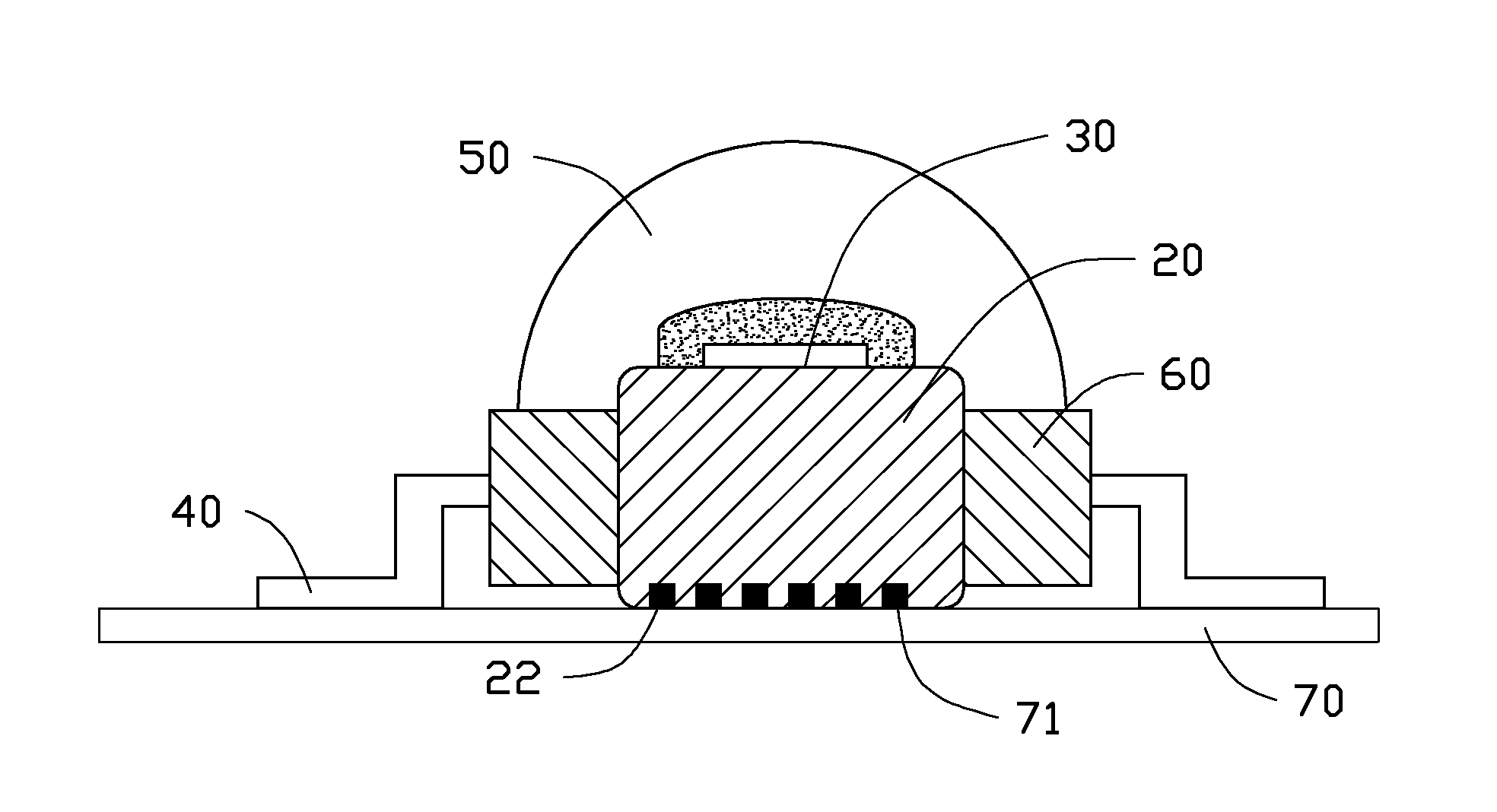
[0027]Referring to FIGS. 5 and 6, the LED chip 30 of an LED package 13 in accordance with the present disclosure is a vertical type LED chip. A bottom of the LED chip 30 is directly connected to an electrode 40 to accomplish an electrical connection. A top of the LED chip 30 is electrically connected to another electrode 40 via a metal wire 42. A plurality of electrically conductive holes 24 and heat conductive holes 25 are defined in the base 20, and electrically conductive materials and heat conductive materials are respectively received in the electrically conductive holes 24 and heat conductive holes 25. Specially, a density of the heat conductive holes 25 around the LED chip 30 is higher than that at other positions. Thus, heat generated by the LED chip 30 can be dissipated more efficiently.

sixth embodiment

[0028]Referring to FIGS. 7 and 8, the LED chip 30 of an LED package 14 in accordance with the present disclosure is mounted on the base 20 by a flip chip technique. The LED chip 30 connects the electrodes 40 for obtaining electrical power. One of the heat conductive holes 25 in the base 20 has a square shape in a top view, and a cross section of the heat conductive hole 25 is trapeziform.


PUM


Abstract

An exemplary LED module includes a board and an LED package mounted on the plate. The LED package includes a base, an LED chip mounted on a top surface of the base, two electrodes formed on the base and electrically connected to the LED chip and the board, and an encapsulant encapsulating the LED chip. A plurality of grooves are defined in the bottom surface of the base. When the LED package is secured on the plate via solder paste, the grooves function as a container for receiving excessive solder paste, thereby preventing the solder paste from spilling and floating or inclination of the LED package.

Description

BACKGROUND[0001]1. Technical Field[0002]The present disclosure relates generally to light emitting devices, and more particularly to a light emitting diode (LED) package and an LED module having the LED package.[0003]2. Description of Related Art[0004]LEDs are solid state light emitting devices formed of semiconductors, which are more stable and reliable than other conventional light sources such as incandescent bulbs. Thus, LEDs are being widely used in various fields such as numeral / character displaying elements, signal lights, light sources for lighting and display devices. When in use, providing LEDs in packages can provide protection, color selection, focusing and the like for light emitted by the LEDs.[0005]A typical LED package includes a base with an LED chip encapsulated thereon. The LED package is generally formed as a surface mounting type device for facilitating application, whereby the base is mounted on a printed circuit board or other similar elements. Solder paste su...

Claims


Application Information

Patent Timeline
Patent Type & Authority Applications(United States)
IPC IPC(8): H01L33/48
CPCH01L33/486H01L33/62H01L33/642H01L2224/48091H01L2924/00014
Inventor CHAN, SHIUN-WEIKE, CHIH-HSUNLO, HSING-FEN
Owner ADVANCED OPTOELECTRONICS TECH
Why Eureka
Try Eureka