Microbolometer infrared sensors

a technology of infrared sensors and microbolometers, which is applied in the direction of optical radiation measurement, radiation control devices, instruments, etc., can solve the problems of poor mechanical properties of such thin silicon dioxide films, incompatible with standard semiconductor technologies, and low thermal conductivity of silicon nitrid

Inactive Publication Date: 2002-03-19
TU XIANG ZHENG
View PDF5 Cites 122 Cited by
  • Summary
  • Abstract
  • Description
  • Claims
  • Application Information

AI Technical Summary

Benefits of technology

Another feature of the microbolometer infrared sensor provided by the present invention is that the microbridge and its supports have higher mechanical strength and lower residual stress.
Still another feature of the microbolometer infrared sensor provided by the present invention is that the microbridge and its supports have lower thermal conductance or higher thermal resistance.
Still another feature of the microbolometer infrared sensor provided by the present invention is that the microbridge and its supports are separated from the substrate by a narrower gap so that they are forced to touch the substrate without damage.

Problems solved by technology

This limits the thickness of a silicon dioxide film to be less than 2 .mu.. Actually, the thickness of silicon dioxide films used in standard integrated circuits is about 1 .mu.. Microstructures of such thin silicon dioxide films have very poor mechanical properties.
1. Patterning a silicon nitride film formed on the surface of a silicon substrate creates steps on the surface of the substrate. Thicker the silicon nitride films higher the steps. This is not compatible with standard semiconductor technologies.
2. The thermal conductivity of silicon nitride is not quite low. It is not suitable for the use as a thermal insulating material.
Common problems with microbolometer infrared sensors based on silicon oxide or silicon nitride are not only to have poor mechanical strength, but also to have difficulties with processing.
It can not be performed after processing the integrated circuits.

Method used


Image

  • Microbolometer infrared sensors
  • Microbolometer infrared sensors
  • Microbolometer infrared sensors

Examples


Embodiment Construction

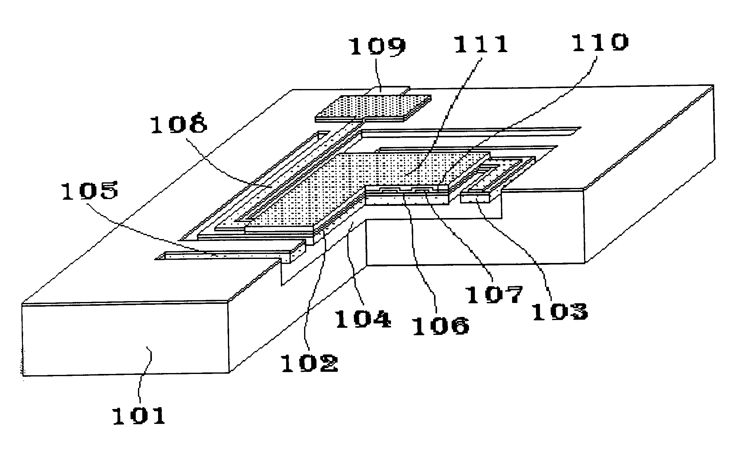
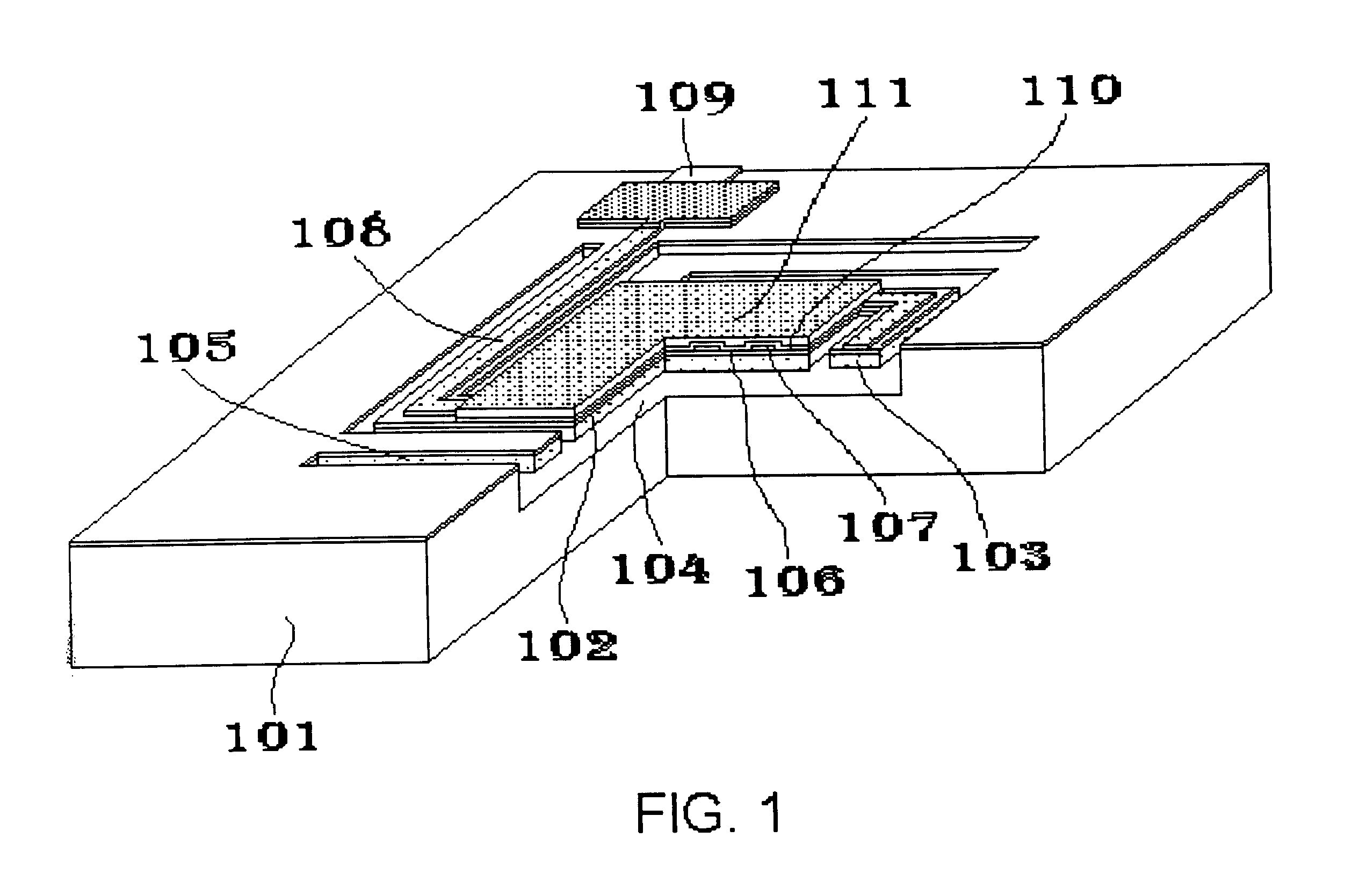
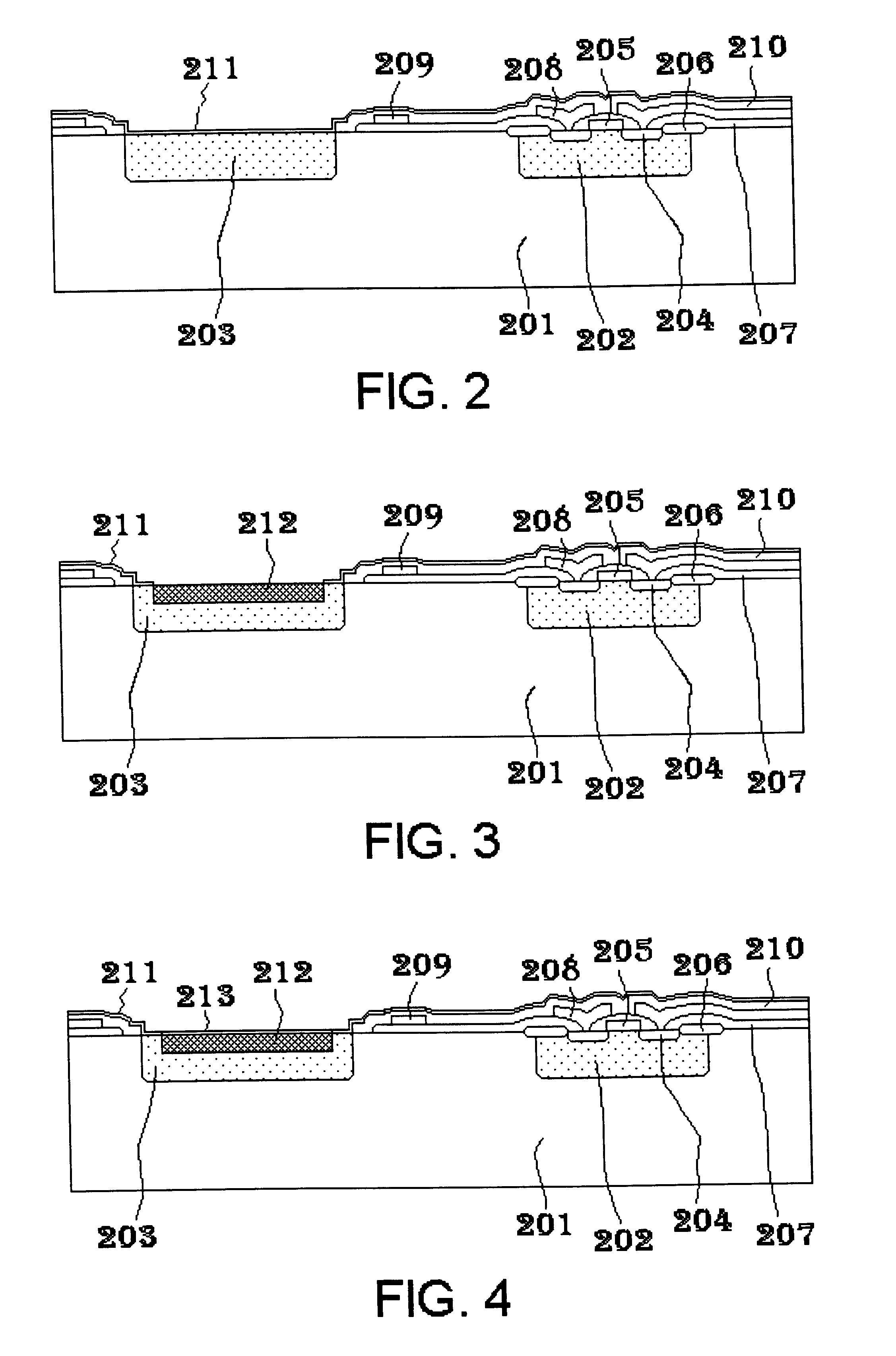
In according to the present invention, a microbolometer infrared sensor array is disposed in a silicon substrate in which there already exists a CMOS circuit with readout electronics. Each microbolometer infrared sensor includes a porous silicon membrane bridging a cavity recessed into the substrate. The porous silicon membrane has four porous silicon beams. The distal ends of the porous silicon beams are anchored to the substrate, so that the porous silicon membrane is supported by the substrate and the surface of the porous silicon beams is aligned with the plane surface of the substrate. The surface of the porous silicon membrane and beams is coated with silicon dioxide film. A temperature sensitive resistor is disposed on the surface of the silicon dioxide film. The end portions of the resistor are disposed on the porous silicon beams and keep in contact with the proximal end portions of electrical conductors which already exist on the surface of the substrate. The surface of th...


PUM

PropertyMeasurementUnit
sheet resistanceaaaaaaaaaa
porosityaaaaaaaaaa
compressive stressaaaaaaaaaa

Abstract

A microbolometer infrared sensor utilizes a porous silicon bridge as its thermal isolating and mechanical supporting structure. Porous silicon formed from single crystal silicon on lightly doped p-type silicon has a thermal conductivity lower than silicon dioxide and silicon nitride, and, therefore, when used as a mechanical supporting structure, can offer better thermal isolation performance. The porous silicon layer can be fabricated much thicker than silicon dioxide and silicon nitride membranes since there is almost no residual stress therein. A thicker porous silicon bridge has higher mechanical support strength. The porous silicon process is a low temperature process. It facilitates a fabrication strategy of microelectronics first and micromechanics last.

Description

This application claims the benefit of China patent application Serial No. 98120652.2, filed on Oct. 21, 1998, and entitled "Microbolom Infared Sensors," and naming Xiang Zheng Tu as inventor.1. Field of the InventionThe invention relates to a microbolometer infrared sensor. Particularly, the invention relates to a microbolometer infrared sensor utilizing a porous silicon bridge as its thermal isolating and mechanical supporting structure.2. Description of the Related ArtMicrobolometer infrared sensors have a wide variety of applications, ranging from security night sights and driving aids to area surveillance, fire-fighting, industrial radiometry, search and rescue, border patrol and vehicle collision avoidance.Newly developed microbolometer infrared sensors are fabricated based on integrated circuit fabricating techniques and micromachining techniques. This type of microbolometer infrared sensors can operate at room temperature without the need for cryocooling, which improves sens...

Claims


Application Information

Patent Timeline
Patent Type & Authority Patents(United States)
IPC IPC(8): H01L27/146G01J5/20
CPCG01J5/20H01L27/14609H01L27/14689H01L27/14649H01L27/14632
Inventor TU, XIANG ZHENG
Owner TU XIANG ZHENG
Why Eureka
Try Eureka