Active matrix substrate, liquid crystal panel, liquid crystal display device, liquid crystal display unit, and television receiver

a technology of liquid crystal display device and active matrix substrate, which is applied in the direction of electric digital data processing, instruments, computing, etc., can solve the problems of difficult to achieve high-quality display and complete prevent the inflow of electric charge, and suppress the occurrence of image sticking of sub-pixels, etc.

Inactive Publication Date: 2012-04-12
SHARP KK
View PDF8 Cites 14 Cited by
  • Summary
  • Abstract
  • Description
  • Claims
  • Application Information

AI Technical Summary

Benefits of technology

[0023]As described above, in a liquid crystal display device using the present active matrix substrate, it is possible to discharge (refresh) an electric charge accumulated in a pixel electrode capacitively coupled to a pixe

Problems solved by technology

It is therefore impossible to completely prevent the inflow of the elect

Method used


Image

  • Active matrix substrate, liquid crystal panel, liquid crystal display device, liquid crystal display unit, and television receiver
  • Active matrix substrate, liquid crystal panel, liquid crystal display device, liquid crystal display unit, and television receiver
  • Active matrix substrate, liquid crystal panel, liquid crystal display device, liquid crystal display unit, and television receiver

Examples


embodiment 1

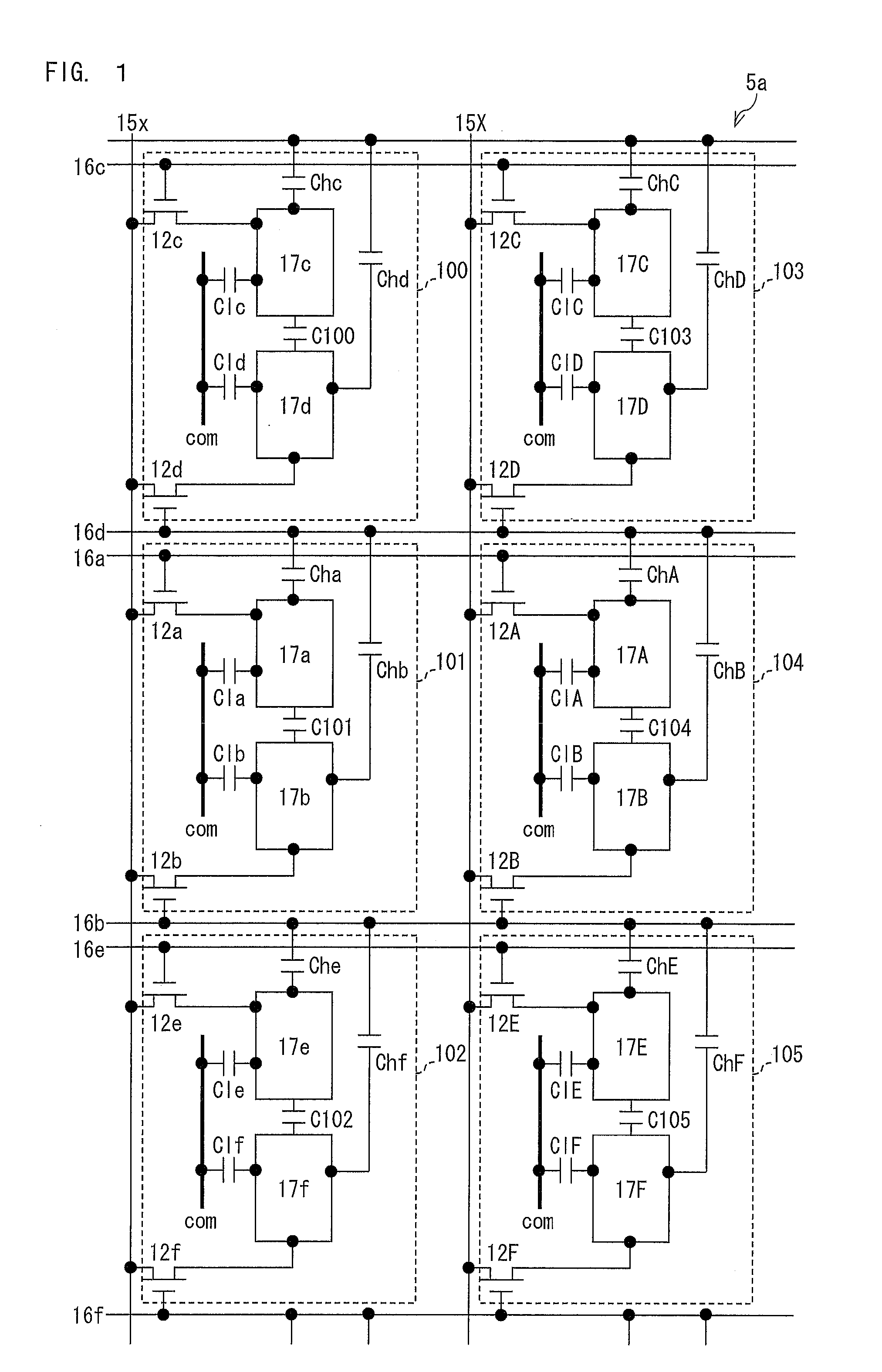
[0075]FIG. 1 is an equivalent circuit diagram illustrating part of the liquid crystal panel of the present Embodiment 1. As shown in FIG. 1, a liquid crystal panel 5a includes data signal lines (15x and 15X) that extend in a column direction (top-to-bottom direction of FIG. 1), scanning signal lines (16a to 16f) that extend in a row direction (left-to-right direction of FIG. 1), pixels (100 to 105) that are disposed in the row and column directions, and a common electrode (counter electrode) com. The pixels have an identical configuration. A pixel array including the pixels 100 through 102 and a pixel array including the pixels 103 through 105 are adjacent each other.

[0076]In the liquid crystal panel 5a, one pixel is associated with one data signal line and two scanning signal lines. Two pixel electrodes 17c and 17d disposed in the pixel 100, two pixel electrodes 17a and 17b disposed in the pixel 101, and two pixel electrodes 17e and 17f disposed in the pixel 102 are arranged in one...

embodiment 2

[0213]FIG. 31 is an equivalent circuit diagram illustrating part of the present liquid crystal panel of the present Embodiment 2. As shown in FIG. 31, a liquid crystal panel 5b includes data signal lines (15x and 15X) that extend in a column direction (top-to-bottom direction of FIG. 31), scanning signal lines (16a to 16f) that extend in a row direction (left-to-right direction of FIG. 31), pixels (100 to 105) that are aligned in the row and column directions, and a common electrode (counter electrode) com. The pixels have an identical configuration. A pixel array including the pixels 100 through 102 and a pixel array including the pixels 103 through 105 are adjacent each other.

[0214]In the liquid crystal panel 5b, one pixel is associated with one data signal line and two scanning signal lines. Three pixel electrodes 17c, 17d, and 17C′ disposed in the pixel 100, three pixel electrodes 17a, 17b, and 17a′ disposed in the pixel 101, and three pixel electrodes 17e, 17f, and 17e′ dispose...


PUM


Abstract

Pixel electrodes (17a and 17b) are provided in a pixel (101), and the pixel (101) is associated with a data signal line (15x), scanning signal lines (16a and 16b), and transistors (12a and 12b). One pixel electrode (17a) is connected to the data signal line (15x) via the transistor (12a). The other pixel electrode (17b) is connected to the pixel electrode (17a) via a capacitor (C101) and is connected to the data signal line (15x) via the transistor (12b). Storage capacitance (Cha and Chb) is formed between the pixel electrodes (17a and 17b) of the pixel (101) and a scanning signal line (16d) associated with a pixel (100). Thus, a configuration of a liquid crystal display device of a capacitively coupled pixel division mode is proposed in which a decline in display quality caused by image sticking of a sub-pixel is less likely to occur.

Description

TECHNICAL FIELD[0001]The present invention relates to an active matrix substrate including a plurality of pixel electrodes in a pixel region, and a liquid crystal display device (pixel division mode) that uses the same.BACKGROUND ART[0002]As a measure for improving viewing angle dependence of gamma characteristics in liquid crystal display devices (for example, holding down excess brightness and the like in a screen), a liquid crystal display device has been proposed which controls a plurality of sub-pixels in a pixel to have different brightness, so as to display a halftone by an area coverage modulation of these sub-pixels (pixel division mode; for example, see Patent Literature 1).[0003]As illustrated in FIG. 48, an active matrix substrate disclosed in Patent Literature 1 has a pixel region provided between two adjacent gate bus lines 112; a pixel electrode 121a is disposed on an upper end (part adjacent to the gate bus line) of the pixel region, a pixel electrode 121b is dispose...

Claims


Application Information

Patent Timeline
IPC IPC(8): G09G3/36G09G5/00G09G3/20
CPCG02F2001/134354G09G3/3659G09G3/3677G09G3/3688G09G2300/0426G02F1/13624G09G2300/0447G09G2300/0876G09G2310/0251G09G2320/0204G09G2320/028G09G2300/0443G02F1/134354
Inventor TSUBATA, TOSHIHIDE
Owner SHARP KK
Why Eureka
Try Eureka