Punch-through diode

a diode and punching technology, applied in the direction of diodes, semiconductor/solid-state device details, instruments, etc., can solve the problems of difficult to fabricate mim diodes having desirable properties, unipolar switching is possible, and unipolar operation may suffer

Active Publication Date: 2012-06-14
SANDISK TECH LLC
View PDF54 Cites 98 Cited by
  • Summary
  • Abstract
  • Description
  • Claims
  • Application Information

AI Technical Summary

Problems solved by technology

However, with a p-i-n diode typically only unipolar switching is possible.
However, unipolar operation may suffer from problems such as requirement of a high RESET current.
However, it can be difficult to fabricate MIM diodes having desirable properties such as a sufficiently high forward bias current.

Method used


Image

  • Punch-through diode
  • Punch-through diode
  • Punch-through diode

Examples


Embodiment Construction

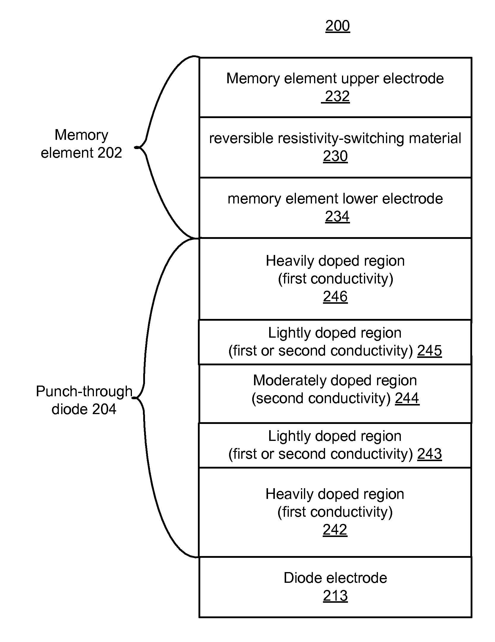
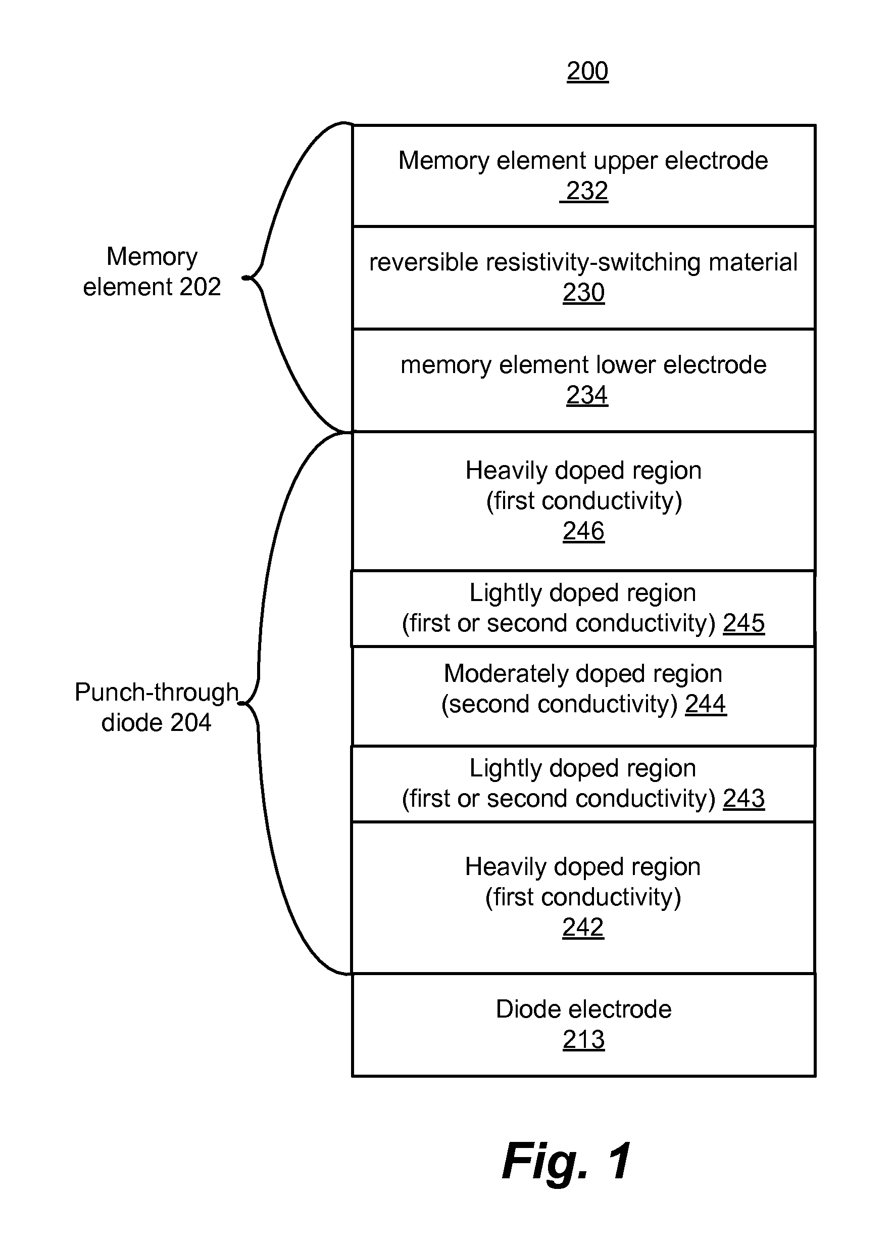
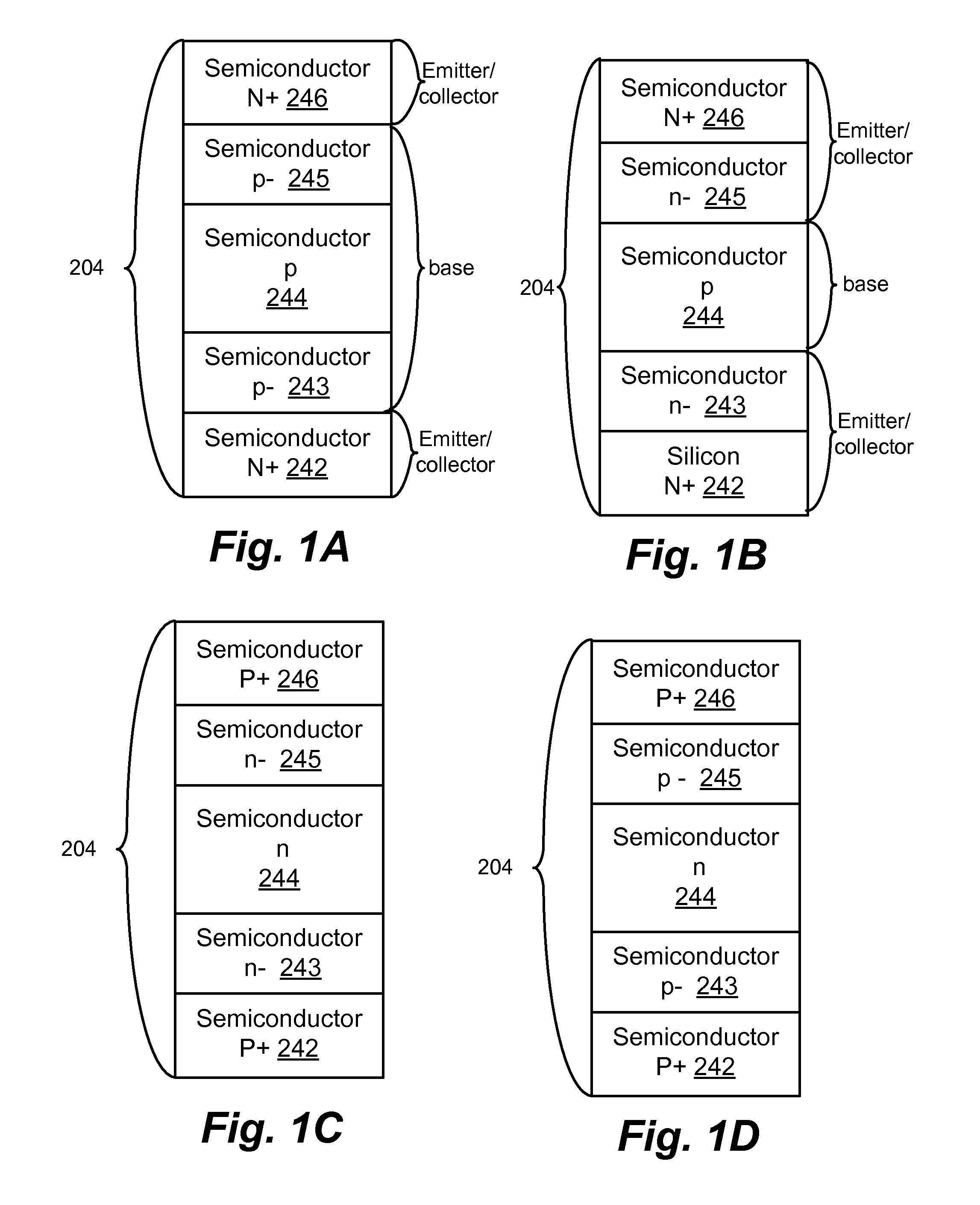
[0029]A punch-through diode and method of fabricating the same are disclosed herein. The punch-through diode may be used as a steering element in a memory device having memory cells with reversible resistivity-switching elements. For example, a memory cell may include a reversible resistivity-switching element in series with a punch-through diode. The punch-through diode allows bipolar operation of a cross-point memory array. The punch-through diode may have a symmetrical non-linear current / voltage relationship. The punch-through diode may have a high current at high bias for selected memory cells and a low leakage current at low bias for unselected memory cells. In other words, the ratio of Ion / Ioff may be high. Therefore, the punch-through diode is compatible with bipolar switching in cross-point memory arrays having resistive switching elements. However, note that embodiments of a punch-through diode disclosed herein may have other applications.

[0030]In one embodiment, the punch-...


PUM


Abstract

A punch-through diode and method of fabricating the same are disclosed herein. The punch-through diode may be used as a steering element in a memory device having a reversible resistivity-switching element. For example, a memory cell may include a reversible resistivity-switching element in series with a punch-through diode. The punch-through diode allows bipolar operation of a cross-point memory array. The punch-through diode may have a symmetrical non-linear current/voltage relationship. The punch-through diode has a high current at high bias for selected cells and a low leakage current at low bias for unselected cells. In other words, the ratio of Ion/Ioff is high. Therefore, the punch-through diode is compatible with bipolar switching in cross-point memory arrays having resistive switching elements.

Description

BACKGROUND[0001]1. Field[0002]This disclosure relates to technology for non-volatile data storage.[0003]2. Description of the Related Art[0004]A variety of materials show reversible resistivity-switching behavior, and as such may be suitable for use as memory elements. One type of material having reversible resistivity-switching behavior is referred to as resistance change memory (ReRAM). Transition metal oxides have been proposed for ReRAM. A second type of material having reversible resistivity-switching behavior is referred to as phase change memory (PCRAM). Chalcogenides, which may change between a crystalline state (conductor) and an amorphous state (insulator), have been proposed for PCRAM. Other materials such as carbon polymers, perovskites, and nitrides have also been proposed as memory elements having reversible resistivity-switching behavior.[0005]Upon application of sufficient voltage, current, or other stimulus, the reversible resistivity-switching material switches to ...

Claims


Application Information

Patent Timeline
Patent Type & Authority Applications(United States)
IPC IPC(8): H01L45/00H01L21/02H01L21/331H01L29/861
CPCH01L29/6609H01L29/66121H01L29/861H01L45/04H01L27/0255H01L45/146H01L27/2409H01L27/2481H01L45/1233G11C2213/72G11C2213/74H10B63/20H10B63/84H10N70/20H10N70/826H10N70/8833
Inventor RABKIN, PETERMIHNEA, ANDREI
Owner SANDISK TECH LLC
Why Eureka
Try Eureka