
MLC Self-RAID Flash Data Protection Scheme

a data protection scheme and self-raid technology, applied in the direction of digital storage, memory adressing/allocation/relocation, instruments, etc., can solve the problems of long delay between operations, limiting the use of read/write capabilities, and generating unpredictable consequences from power interruptions

Active Publication Date: 2012-10-18
SANDISK TECH LLC
View PDF11 Cites 0 Cited by
  • Summary
  • Abstract
  • Description
  • Claims
  • Application Information

AI Technical Summary

Benefits of technology

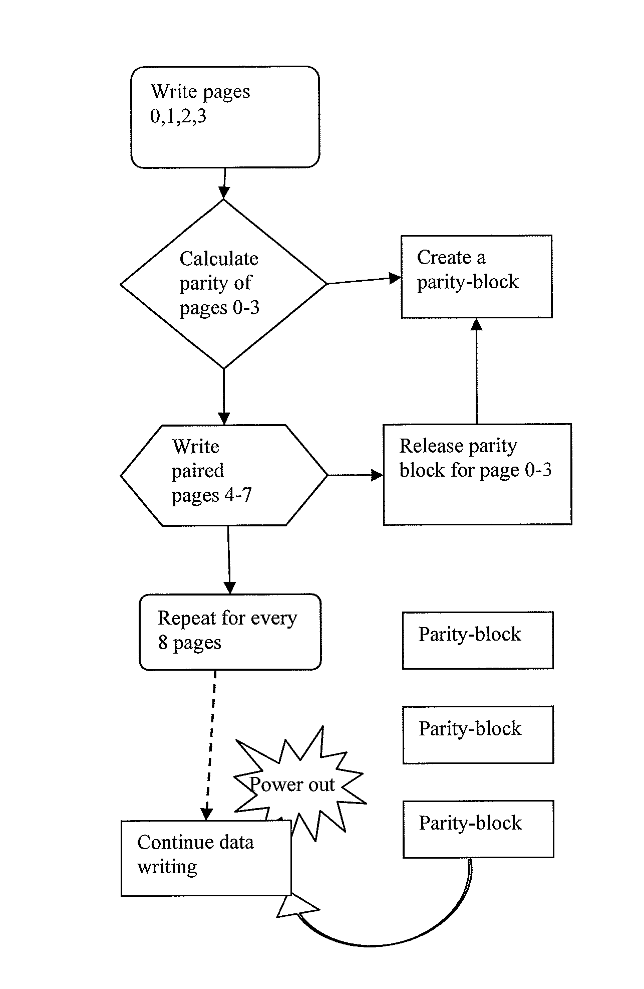
[0021]The present invention provides a method of preserving page-based flash memory integrity during writing, in the event of a power loss. The present invention can be used to manage a flash memory having multiple level cells (MLC).
[0025]According to the present invention, a method for reducing data corruption from device wearing out is provided by extending the programming and erasing time on selected weak cells. Weak cells are identified by the rate they generate errors, and then the blocks and pages associated with the weak cells can be programmed and erased at a slower rate than other cells. By tracking the weaker blocks and treating them differently than other more robust blocks, endurance can be enhanced. Because the slower programming and erasure processes are only performed on the relatively few weak blocks, overall performance is not significantly compromised. A method of managing a multiple level cell flash memory with numerous pages, the method comprising: (a) programming and erasing data on a page at a predetermined speed; (b) detecting an error rate for each of the pages and identifying the pages associated with error rates that exceed a predetermined value; (c) programming and erasing the identified high error page set a speed that is slower than the predetermined speed.
[0026]According to another embodiment of the present invention, a method for overcoming the leakage induced charge level shifts is provided. A method of managing a multiple level cell flash memory that includes a sense circuitry, the method comprising: (a) selecting a sense voltage; (b) detecting charge levels of memory cells in the multiple level cell flash memory with the selected sense voltage, and making a first table that correlates the predetermined sense voltage and the sensed charge levels; (c) reducing the sense voltage and detecting charge levels of memory cells in the multiple level cell flash memory using the reduced sense voltage and making a second table that correlates the reduced sensed voltage with the sensed charge levels; (d) replacing the first table with the second table.

Problems solved by technology

The constraints of the head / media technology limit the read / write capabilities to using only one active head at a time.
All data requests that are sent to the drive are handled in a serial manner, with long delays between operations, as the actuator moves the read / write head to the required position and the media rotates to place the data under the read / write head.
As a result, multiple data bits that share the same cell and their electronic states, (hence their threshold voltage Vt's), are interdependent to a point that an unexpected power interruption can generate unpredictable consequences.
In spite of the advantages of MLC over SLC, MLC flash memory devices have not traditionally been used because of certain technical constraints, among which data corruption presents one of the most severe challenges.
MLC flash memory devices are more vulnerable to data corruption than SLC flash memory devices.
The lower cycle limit in the MLC flash memory devices poses particular problems for data centers that operate with unpredictable data streams.
The unpredictable data streams may cause “hot spots”, resulting in certain highly-used areas of memory being subject to a large number of erase cycles.
In addition, various factors in normal operation can also affect flash memory integrity, including read disturbs or program disturbs.
These disturbs lead to unpredictable loss of data bits in a memory cell, as a result of the reading or writing of memory cells adjacent to the disturbed cell.
Sudden data losses in MLC flash memory devices due to unexpected power interruptions require frequent data recoveries.
Because some data levels require more than one write operations to achieve and because more than one bit of data share the same memory cell, a power change or a program error during a write data operation leaves the data in a wrong state.
When the power returns, the memory cell can be in an erratic state.
Therefore a power interruption is a major risk to the integrity of data stored in MLC flash memory devices.
If the power failure occurs while the MLC is in the middle of an operation that changes the contents of the flash media (e.g., in the middle of writing a page of data or in the middle of erasing a block of data), the electrical states of the interrupted page or block are unpredictable after the device is powered up again.
However, other bits may be lagging behind and have not yet reached their target values yet.
Furthermore, some bits might be caught in intermediate states and thus be in an unreliable mode, so that reading these bits returns different results under different read operations.
Therefore power losses while programming a certain page can corrupt a paired page.
Those techniques require either additional memory or complicated error-searching and data rebuilding procedures after power returns.
Such requirements or solutions make the process costly to implement and place significant strain on the processing power of a conventional flash memory controller, which generally includes only a single processor.
Furthermore, if a power failure occurs during the writing of a page, the paired page data can become corrupt in a MLC flash memory device.
Therefore even the conventional paired page technique is susceptible to a sudden power interruption.
As a matter of fact, the severity of the possible corruption is high; in some cases, every 10th data bit can be lost.
Relying on conventional ECC techniques to make a MLC flash memory system reliable would be impractical to implement.
NAND flash memory data corruption can also result from program erase cycle wear outs.
Repeated program / erase cycles damage the oxide and reduce its effectiveness.
As device dimensions (e.g., oxide film thickness) shrink, data integrity problems from device wearing out can become more severe.
One factor that influences this wearing out process is the speed at which the program and erase cycles are performed.
However, if the speed of programming and erasing is slowed to avoid wearing out, overall performance can be impacted significantly.
However, as the device wears out, its ability to store a charge is compromised.
However, a lower sense voltage also returns a lower detected voltage, thus resulting in an incorrect charge tracking.

Method used


Image

  • MLC Self-RAID Flash Data Protection Scheme
  • MLC Self-RAID Flash Data Protection Scheme
  • MLC Self-RAID Flash Data Protection Scheme

Examples


Embodiment Construction

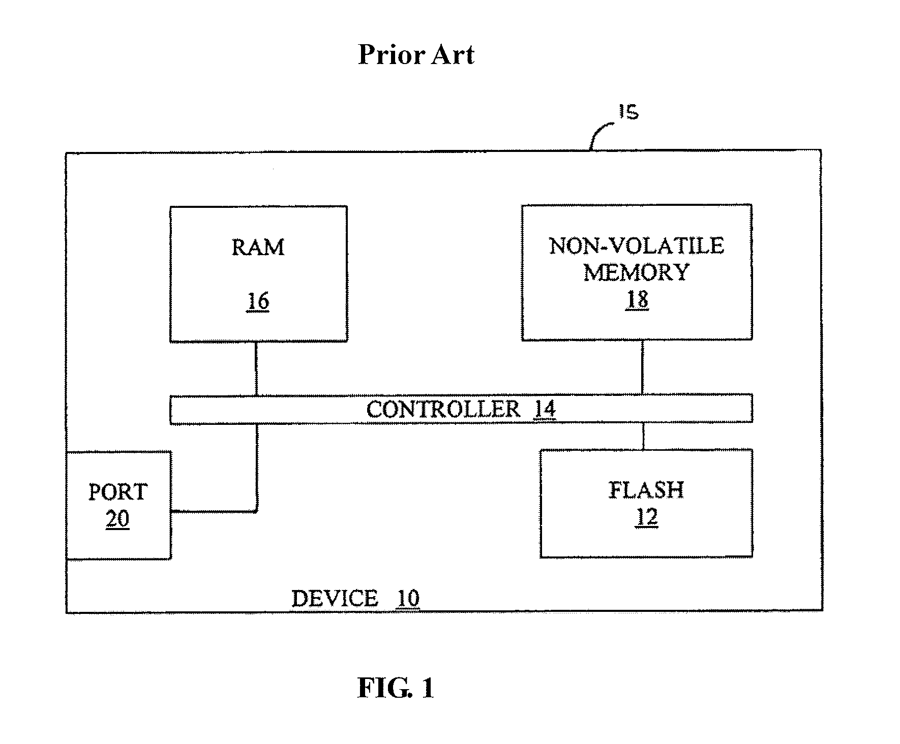
[0042]FIG. 1 is a high level schematic block diagram of a conventional NAND flash media device in a non-volatile data storage unit.

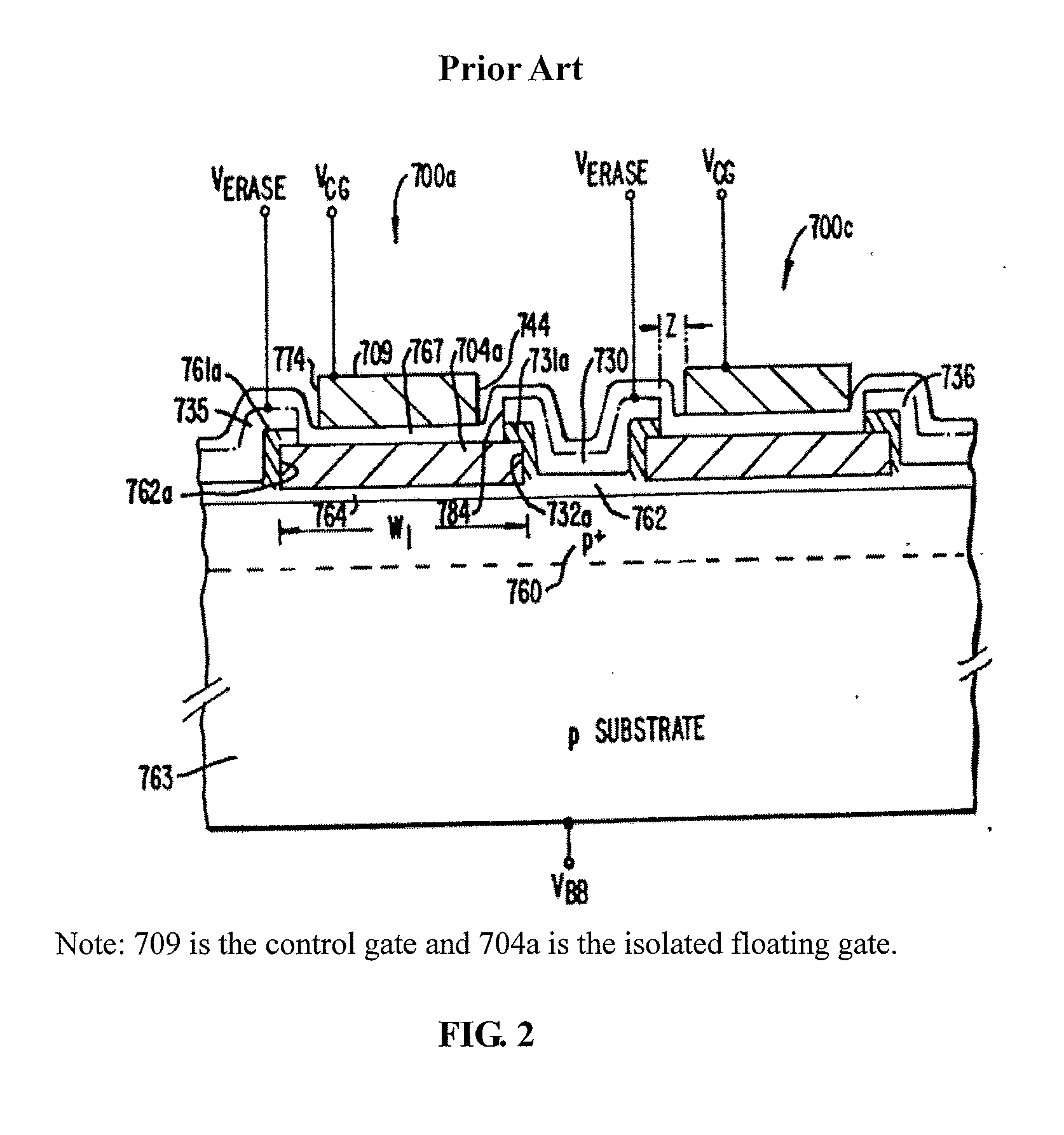
[0043]FIG. 2 shows a cross sectional view of a conventional flash memory device.

[0044]An example of a conventional multiple level (MLC) flash memory cell is illustrated in FIG. 3, where a split channel device has two different threshold voltages, Vt1 and Vt2. The referenced cross sectional view and equivalent circuit are taken from U.S. Pat. No. 5,045,940 (Harari).

[0045]Variations of the electronic states generate ranges of threshold voltages in a real MLC system. FIG. 4 depicts the threshold voltage spans in a conventional two-bit MLC device.

[0046]Pages of data sharing the same multiple level cells are called “shared pages”. Each manufacturer may use a different distance between its shared pages. Many memory vendors prefer to set the distance at four. For example, at a pair distance of 4, page 0 is paired with page 4, page 1 is paired with page 5, page ...


PUM


Abstract

A two-dimensional self-RAID method of protecting page-based storage data in a MLC multiple-level-cell flash memory device. The protection scheme includes reserving one parity sector across each data page, reserving one parity page as the column parity, selecting a specific number of pages to form a parity group, writing into the parity page a group parity value for data stored in the pages of the parity group. The parity sector represents applying a RAID technique in a first dimension. The group parity represents applying a RAID technique in a second dimension. Data protection is achieved because a corrupted data sector can likely be recovered by the two dimensional RAID data.

Description

CROSS-REFERENCE TO RELATED APPLICATIONS[0001]This application is a divisional of U.S. application Ser. No. 12 / 726,200, filed Mar. 17, 2010, which is incorporated by reference herein its entirety.[0002]This application is related to the following co-pending patent applications: (1) U.S. patent application Ser. No. ______, filed Jun. 27, 2012, (Attorney Docket No. 58752-01-5044-US); and (2) U.S. patent application Ser. No. ______, filed Jun. 27, 2012, (Attorney Docket No. 58752-01-5045-US), which are incorporated by reference herein their entirety.[0003]This application also relates to subject matter in the following co-pending patent applications: U.S. patent application Ser. No. 12 / 082,202, filed on Apr. 8, 2008, entitled “System and Method for Performing Host Initiated Mass Storage Commands Using a Hierarchy of Data Structures”; U.S. patent application Ser. No. 12 / 082,205, filed on Apr. 8, 2008, entitled “Flash Memory Controller Having Reduced Pinout”; U.S. patent application Ser. ...

Claims


Application Information

Patent Timeline
Patent Type & Authority Applications(United States)
IPC IPC(8): G06F11/00G06F12/02
CPCG06F11/1044G11C16/22G06F11/1072G06F11/1012G06F12/02G06F12/16
Inventor OLBRICH, AARON K.PRINS, DOUG
Owner SANDISK TECH LLC
Learn More