Sensor for microscopy

a microscopy and sensor technology, applied in the field of digital scanning microscopes, can solve the problems of limiting the overall throughput time of the scanner, requiring the use of complex and cumbersome mechanical components, and complex and cumbersome actuators for adjusting the focus position of the objective, and achieve the effect of efficient change of focus depth

Active Publication Date: 2012-11-15
KONINKLIJKE PHILIPS ELECTRONICS NV
View PDF2 Cites 30 Cited by
  • Summary
  • Abstract
  • Description
  • Claims
  • Application Information

AI Technical Summary

Benefits of technology

[0017]Thus, according to the invention, a 2D array sensor is caused to act as an x-line sensor by using a limited selection (the sub-array) of its sensing area (the letter ‘x’ here refers to an integer number which as will be seen later is below the total number of lines in the 2D array sensor). Said differently, a 2D array sensor is caused to simulate the functionally and operation of an x-line sensor. And as will become clear herein after, using such a simulated x-line sensor in a scanner arrangement where the cross section of the sample can be imaged by this sensor, allows various advantages such as to overcome the above-mentioned problems. Among others, a scanning imaging system is provided with efficient change of focus depth during scanning.

Problems solved by technology

For instance, the need of such focus maps may limit the overall throughput time of the scanner (the throughput time may typically refer to the overall time needed to output an image of the sample or in certain circumstances to output an image band of this sample) because as explained above, it requires at least one prior step of map generation.
Further, the numerous focus adjustments required with a 1D line sensor may require the use of complex and cumbersome mechanical components to obtain fast and accurate image acquisitions.
For example, complex and cumbersome actuators for adjusting the focus position of the objective during the scanning process may be required.
Further, due to focus errors, sometimes the scanning process itself should be rendered more complex.

Method used


Image

  • Sensor for microscopy
  • Sensor for microscopy
  • Sensor for microscopy

Examples


Embodiment Construction

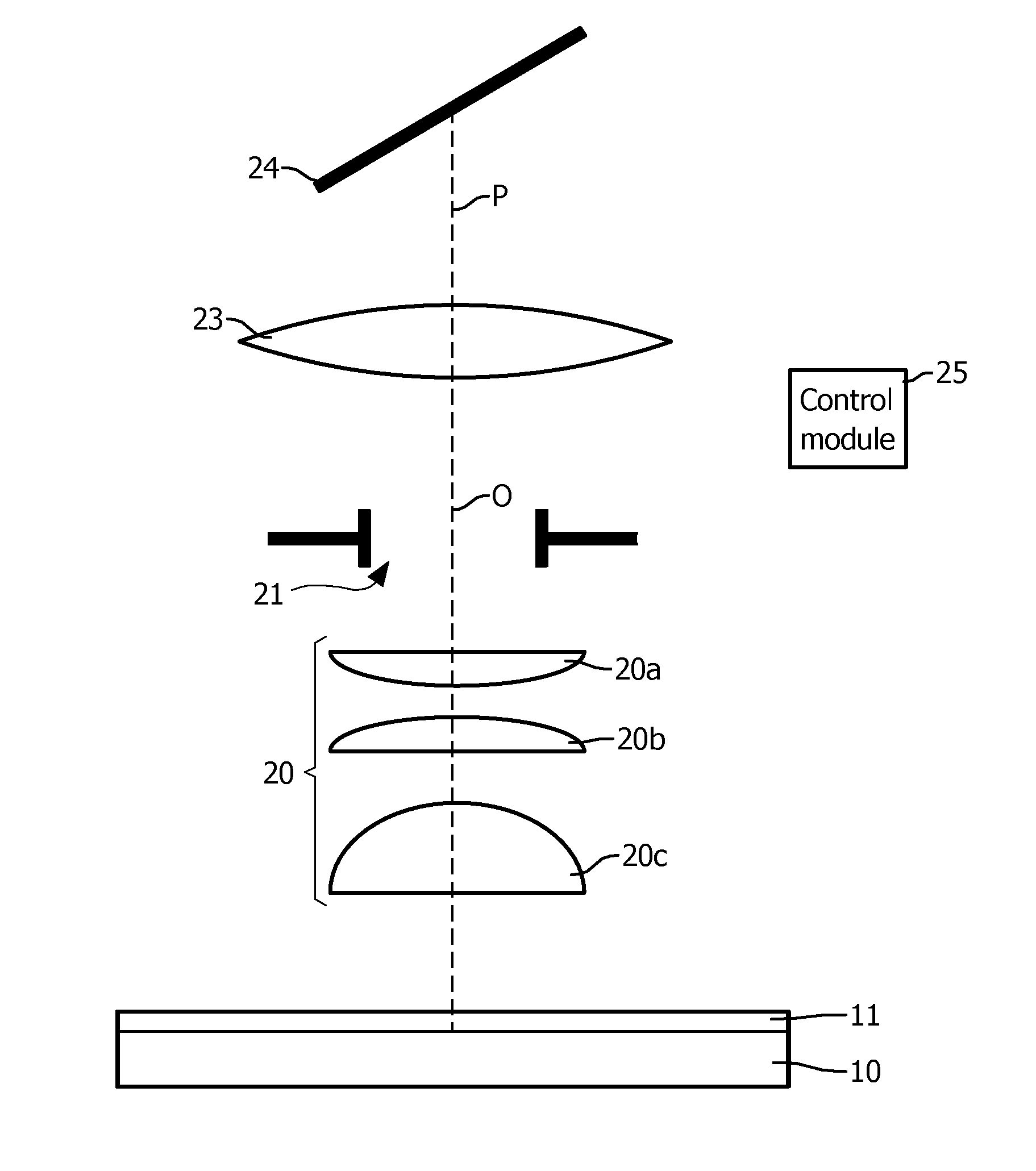
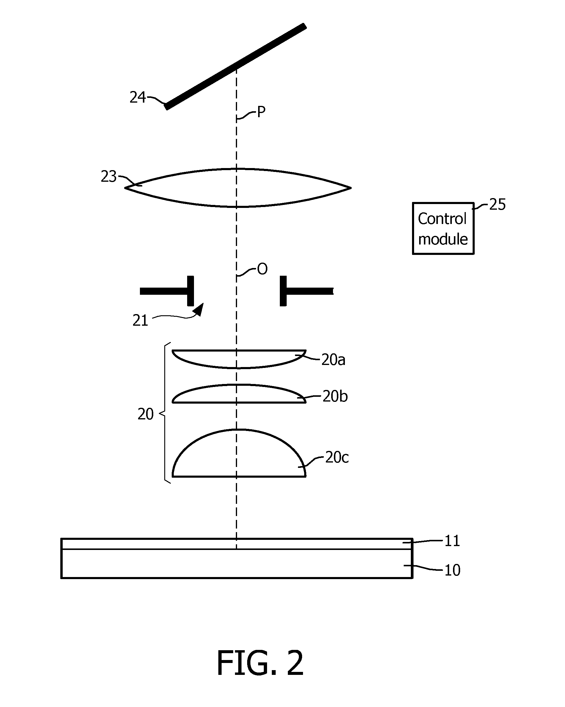
[0036]A scanning microscope according to an embodiment of the invention is illustrated in FIG. 2.

[0037]This scanner is arranged for imaging a sample (e.g. a tissue layer not shown) which can be placed between a glass slide 10 and a cover slip 11.

[0038]Such a microscope slide is placed on a holding surface of a sample holder not shown in the figure.

[0039]As may be known in the art, along an imaging path P and starting from the microscope slide, the scanner may notably comprise a microscope objective 20, typically made of a plurality of lenses 20a, b, and c, an aperture 21 for blocking un-scattered reflected light from the tissue sample, a tube lens 23 and a sensor 24.

[0040]The sensor 24 comprises a 2D array of pixels, also referred herein as matrix of pixels. This sensor is typically a CMOS imaging sensor.

[0041]As can be seen from FIG. 2, the matrix of pixels is tilted with respect to the optical axis O of the microscope objective lens.

[0042]The scanner further comprises a control mo...


PUM


Abstract

This invention pertains to a method for microscopically imaging a sample, with a digital scanner comprising a sensor including a 2D array of pixels and to a digital scanning microscope carrying out this method. It is notably provided a method for microscopically imaging a sample with a scanner comprising a sensor including a 2D array of pixels in an XY coordinate system, the axis Y being substantially perpendicular to the scan direction, wherein the scanner is arranged such that the sensor can image an oblique cross section of the sample, and wherein the method comprises the steps of: • activating a first sub-array of the 2D array of pixels, the first sub-array extending mainly along the Y axis at a first X coordinate (X1), • creating a first image by imaging a first area of the sample by means of the first sub-array of pixels. According to aspects of the invention, it is further proposed a scanner carryout this method and using the same 2D array sensor for imaging and auto-focusing purpose.

Description

FIELD OF THE INVENTION[0001]This invention relates to the field of digital scanning microscopes, and applies advantageously in the field of digital pathology.[0002]In particular this invention relates to a method for microscopically imaging a sample, with a digital scanner comprising a sensor including a 2D array of pixels and to a digital scanning microscope, also called scanner herein after, carrying out this method.BACKGROUND OF THE INVENTION[0003]A digital scanning microscope usually makes a digital image of a sample such as a tissue sample placed in a microscope slide.[0004]This is typically done by scanning the sample over the whole microscope slide and stitching different image bands together and / or by overlaying images measured at different wavelengths.[0005]FIG. 1 schematically represents a cross-section of such a microscope slide. It notably comprises a glass slide 1 with a typical thickness of 1 mm (millimeter), a cover slip 2 with a typical thickness of 0.17 mm, a mounti...

Claims


Application Information

Patent Timeline
Patent Type & Authority Applications(United States)
IPC IPC(8): H04N7/18
CPCG02B21/361G02B21/241G02B21/367
Inventor HULSKEN, BASSTALLINGA, SJOERD
Owner KONINKLIJKE PHILIPS ELECTRONICS NV
Why Eureka
Try Eureka