

Light emitting device array driver circuit and current splitter circuit and method of splitting current therefor
a technology of light emitting devices and driver circuits, which is applied in the direction of static indicating devices, instruments, semiconductor lamp usage, etc., can solve the problems of not operating normally, not properly feedback control the supply voltage, and the emitting device string or string cannot operate normally to emit ligh
- Summary
- Abstract
- Description
- Claims
- Application Information
AI Technical Summary
Benefits of technology
Problems solved by technology
Method used
Image

Examples
first embodiment
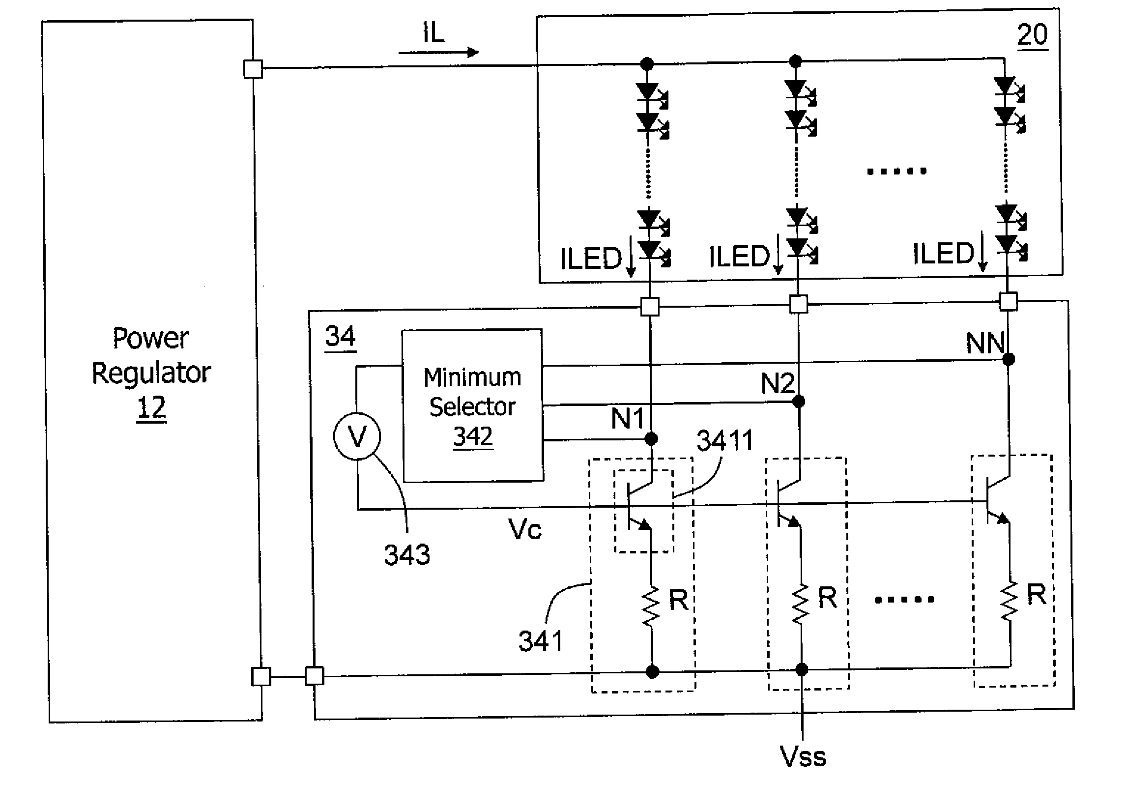
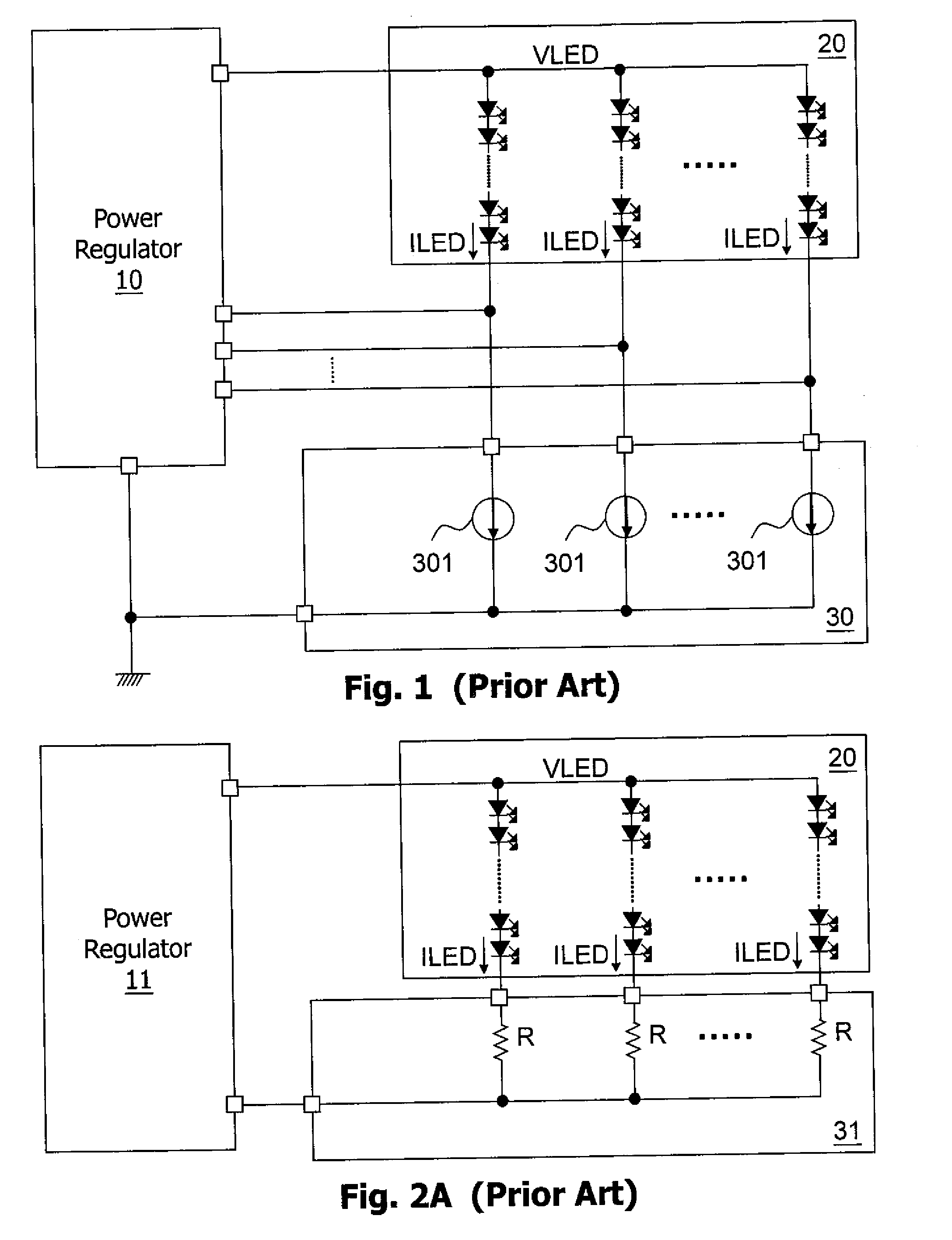
[0059]Please refer to FIG. 3 which shows the present invention. As shown in FIG. 3, a power regulator 12 provides a supply current IL to the light emitting device array 20. The light emitting device array 20 includes multiple light emitting device strings. Each light emitting device string has a first end electrically connected to the power regulator 12 in common, and a second end electrically connected to a first end (nodes N1-NN) of a corresponding current source circuit 341 in a current splitter circuit 34. Besides electrically connected to the first ends of the light emitting device strings the power regulator 12 is also electrically connected to a ground level (Vss) so that a current loop is formed to provide a supply current IL to the light emitting device array 20. One feature of the present invention is that the current splitter circuit 34 includes a minimum selector circuit 342 which senses voltages at the nodes N1-NN and generates a minimum signal indicating a lowest volta...
second embodiment
[0061]FIG. 4A shows the present invention. The current splitter circuit 34 may further comprise a gain circuit 344, which is an amplifier in this embodiment as shown in the figure. The amplifier has a first input coupled to the minimum selector circuit 342 for receiving the minimum signal, and an output which is feedback coupled to its second input. Optionally, a first bias circuit 343 may be provided between the second input and the output for adjusting the current control signal Vc outputted from the gain circuit 344 so that the current source circuit 341 is better controlled as explained in the above. The location of the first bias circuit 343 is not limited to the location as shown in FIG. 4A. Referring to FIG. 4B, the first bias circuit 343 can be provided at any one or more locations shown in the figure; or, the first bias circuit 343 may be omitted, and an inherent bias voltage may be provided between two inputs of the gain circuit 344, or provided in the minimum selector cir...
eighth embodiment
[0064]FIG. 8 shows the present invention, in which the minimum selector circuit 342 and the first bias circuit 343 are shown in more detail as an example. As shown in the figure, the minimum selector circuit 342 includes multiple second bias circuits 3421, coupled between the second ends (nodes N1-NN) of the light emitting device strings and a node B respectively. In this embodiment, the second bias circuit 3421 for example can be a diode having a cathode coupled to the second end of the corresponding light emitting device string, and thus the voltage at the node B will be the lowest voltage among the nodes N1-NN plus the voltage across the diode. The second bias circuit 3421 is not limited to the diode as shown; it can be embodied as other devices, which will be described later.
[0065]In this embodiment, the first bias circuit 343 includes a third bias circuit 3431, a fourth bias circuit 3433, and circuit devices 3432 and 3434. One end of the third bias circuit 3431 is coupled to th...
PUM
 Abstract
Description
Claims
Application Information