Drive method of el display panel

a display panel and drive method technology, applied in static indicating devices, instruments, organic semiconductor devices, etc., can solve the problems of difficult to implement a large high-resolution display panel of the former type, display irregularities, and difficult control methods, etc., to achieve uniform display

Active Publication Date: 2005-08-04
JAPAN DISPLAY CENT INC
View PDF31 Cites 250 Cited by
  • Summary
  • Abstract
  • Description
  • Claims
  • Application Information

AI Technical Summary

Benefits of technology

[0013] In view of the above problems with conventional EL elements, an object of the present invention is to provide a drive method of an EL display apparatus which can achieve more un

Problems solved by technology

It is difficult to implement a large high-resolution display panel of the former type although the former type is simple in structure and inexpensive.
The latter type allows a large high-resolution display panel to be implemented, but involves a problem th

Method used


Image

  • Drive method of el display panel
  • Drive method of el display panel
  • Drive method of el display panel

Examples


Embodiment Construction

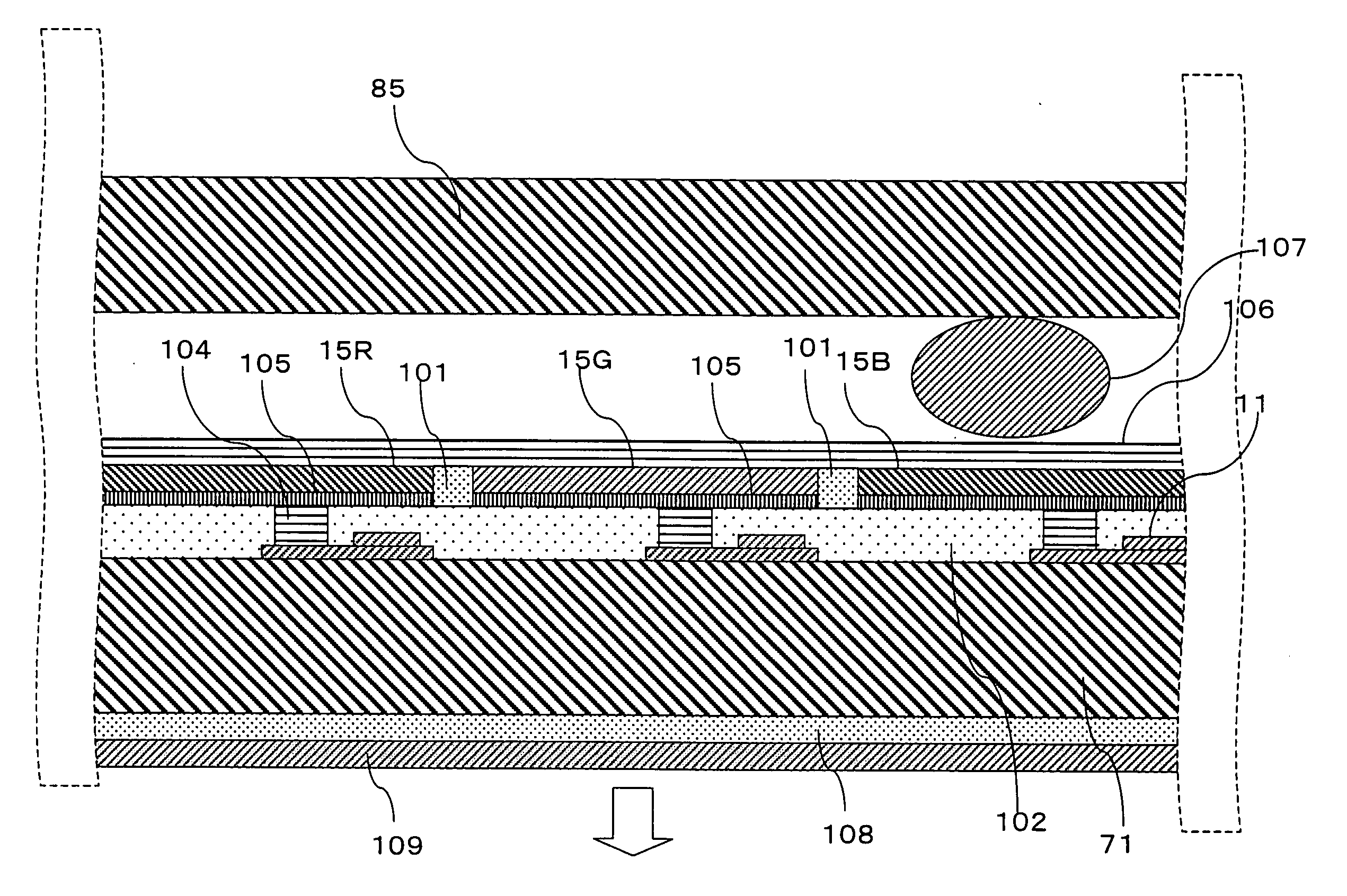
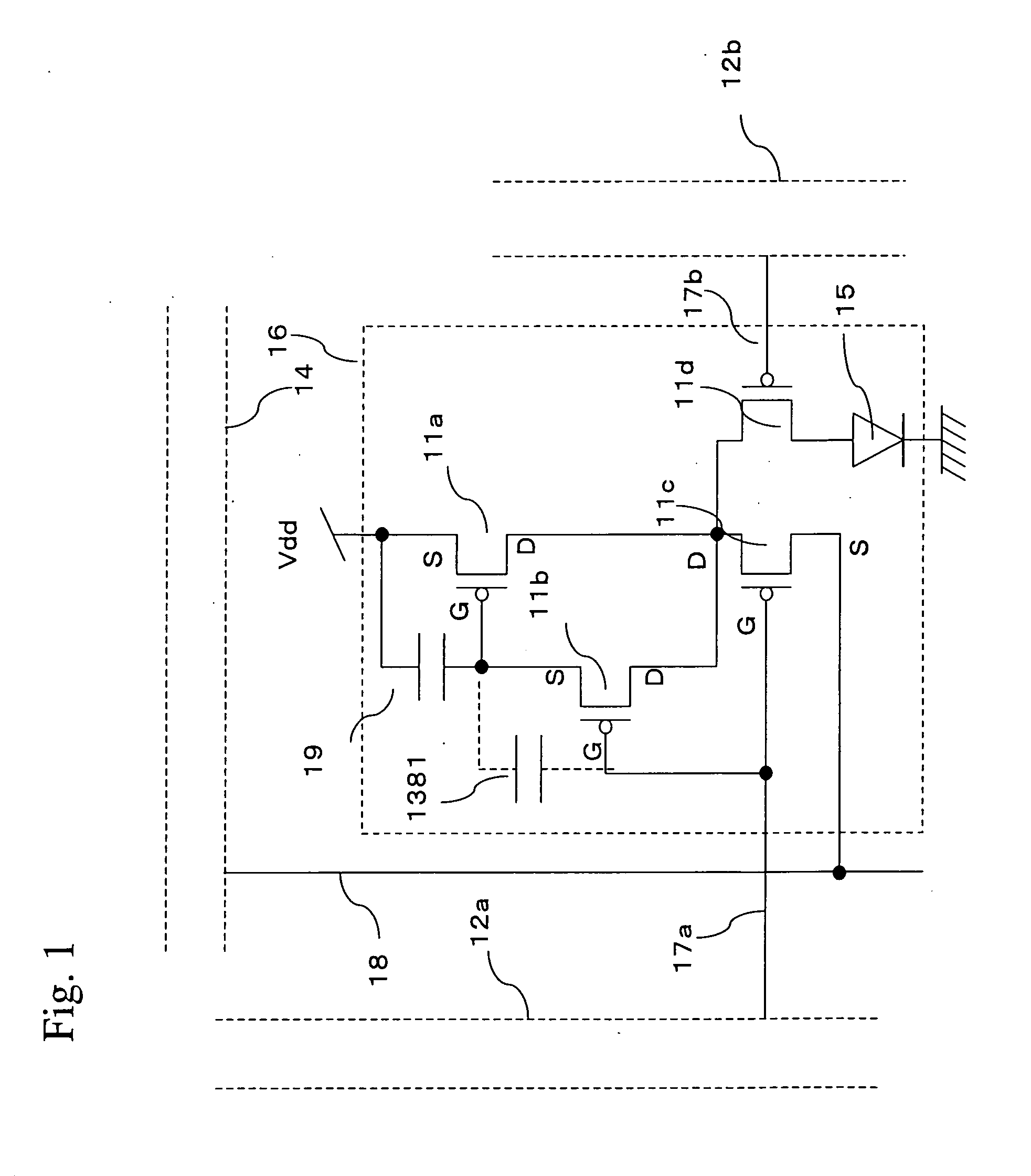
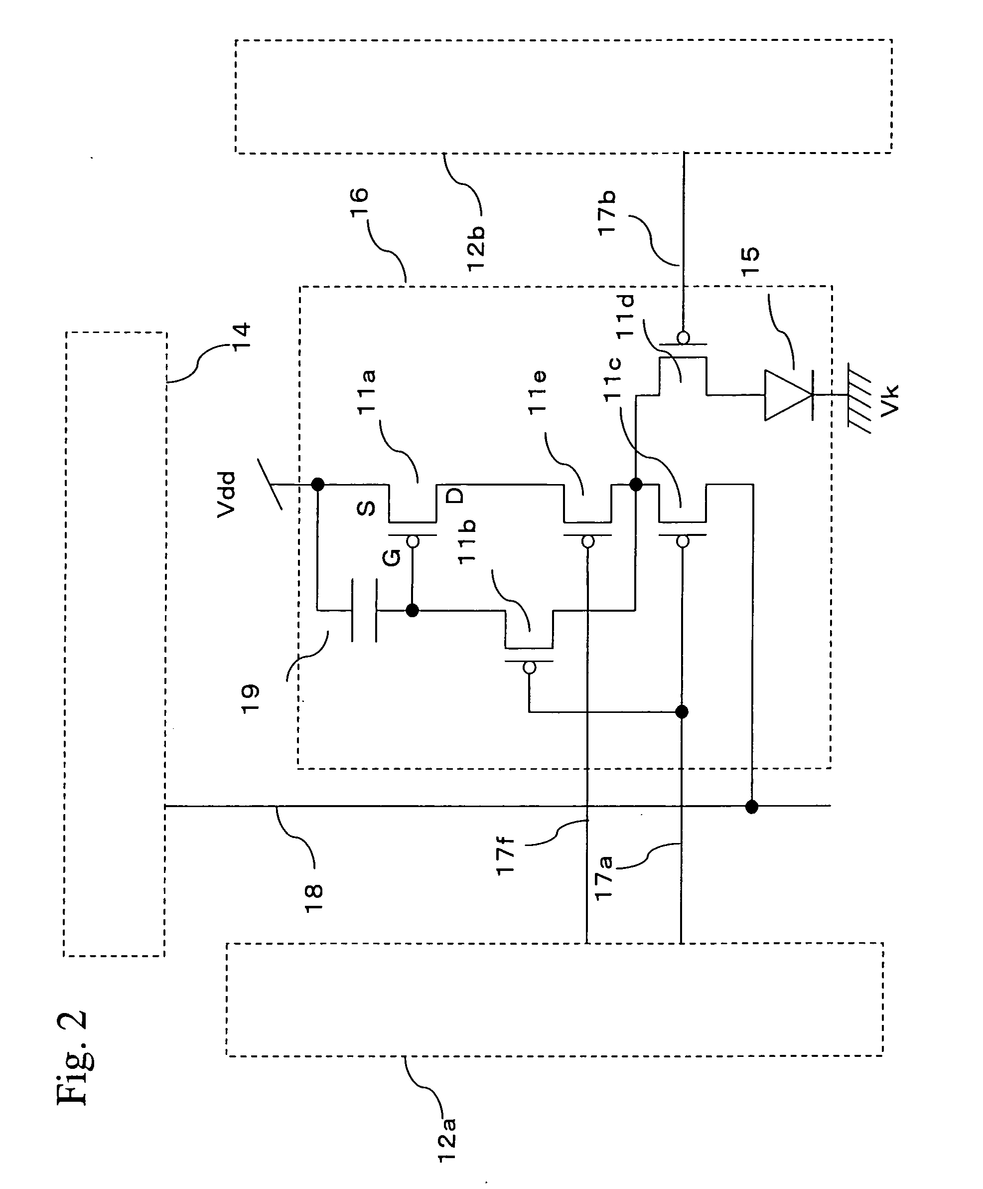
[0416] Some parts of drawings herein are omitted and / or enlarged / reduced herein for ease of understanding and / or illustration. For example, in a sectional view of a display panel shown in FIG. 11, a encapsulation film 111 and the like are shown as being fairly thick. On the other hand, in FIG. 10, a sealing lid 85 is shown as being thin. Some parts are omitted. For example, although the display panel according to the present invention requires a polarizing plate of a phase film such as a circular polarizing plate to prevent reflection, the phase film is omitted in drawings herein. This also applies to the drawings below. Besides, the same or similar forms, materials, functions, or operations are denoted by the same reference numbers or characters.

[0417] Incidentally, what is described with reference to drawings or the like can be combined with other examples or the like even if not noted specifically. For example, a touch panel or the like can be attached to a display panel in FIG....


PUM


Abstract

In order to charge and discharge parasitic capacitance of a source signal line sufficiently and program a predetermined current value into a pixel transistor, it is necessary to output a relatively large current from the source driver circuit.
However, if such a large current is passed through the source signal line, the value of this current is programmed into the pixel, causing a larger than desired current to flow through an EL element 15.
For example, if a 10 times larger current is used for programming, a 10 times larger current flows through the EL element 15, and thus the EL element 15 illuminates 10 times more brightly. To obtain predetermined emission brightness, the time during which the current flows through the EL element can be reduced to 1/10 of one frame (1 F). This way, the parasitic capacitance of the source signal line can be charged and discharged sufficiently and the predetermined emission brightness can be obtained.

Description

TECHNICAL FIELD [0001] The present invention relates to a self-luminous display panel such as an EL display panel which employs organic or inorganic electroluminescent (EL) elements. Also, it relates to an information display apparatus and the like which employ the EL display panel, a drive method for the EL display panel, and the drive circuit for the EL display panel. BACKGROUND ART [0002] Generally, active-matrix display apparatus display images by arranging a large number of pixels in a matrix and controlling the light intensity of each pixel according to a video signal. For example, if liquid crystals are used as an electrochemical substance, the transmittance of each pixel changes according to a voltage written into the pixel. Even with active-matrix display apparatus which employ an organic electroluminescent (EL) material as an electrochemical substance, the basic operation is the same as in the case of using liquid crystals. [0003] In a liquid crystal display panel, each pi...

Claims


Application Information

Patent Timeline
IPC IPC(8): G09G3/00G09G3/20G09G3/22G09G3/32H01L27/32H01L51/52
CPCG09G3/006G09G2320/08G09G3/2014G09G3/22G09G3/3241G09G3/325G09G3/3266G09G3/3283G09G2300/0408G09G2300/0417G09G2300/0452G09G2300/0809G09G2300/0842G09G2300/0861G09G2300/0866G09G2310/02G09G2310/0218G09G2310/0251G09G2310/0256G09G2310/0262G09G2310/027G09G2310/0283G09G2310/0297G09G2310/06G09G2310/061G09G2320/0214G09G2320/0223G09G2320/0233G09G2320/0261G09G2320/043G09G2320/0606G09G2320/0626G09G2320/066G09G2330/02G09G2330/12H01L27/3211H01L27/3213H01L27/3223H01L27/3244H01L51/5237H01L51/5262H01L51/5281H01L51/529H01L2251/568G09G3/20H10K59/351H10K59/88H10K59/353H10K59/12H10K59/131H10K50/846H10K50/85H10K50/87H10K50/844H10K50/86H10K71/861G09G3/30H05B33/14G09G3/32
Inventor TAKAHARA, HIROSHITSUGE, HITOSHI
Owner JAPAN DISPLAY CENT INC
Why Eureka
Try Eureka