Liquid crystal display with superposed contact holes and method of manufacturing the same

Active Publication Date: 2006-10-31
NEC LCD TECH CORP
View PDF5 Cites 10 Cited by
  • Summary
  • Abstract
  • Description
  • Claims
  • Application Information

AI Technical Summary

Benefits of technology

[0022]By employing the foregoing structure, in the IPS liquid crystal display in which the signal lines are partially covered with the common electrode via the interlayer insulating film, the probability of occurrence of short-circuiting between the signal lines and the common electrode via the contact holes connecting the common wiring and the common electrode to each other can be lowered to thereby enable improvement in manufacturing yield. Further, since the contact holes are arranged in zigzags, the uniformity of display can be ensured.
[0023]Further, when the interlayer insulating film is formed only by the inorganic insulating films, the inorganic insulating films are formed by performing the film forming process twice and the contact hole forming process is also carried out twice. As a consequence, even if pinholes are generated in the inorganic insulating films due to dry etching implemented upon forming the contact holes, the pin holes do not go through the total thickness of the inorganic insulating films. Therefore, the probability of occurrence of short-circuiting between the signal

Problems solved by technology

In the foregoing IPS liquid crystal display in which the signal lines are partially covered with the common electrode via the interlayer insulating film, however, when pinholes are generated in th

Method used


Image

  • Liquid crystal display with superposed contact holes and method of manufacturing the same
  • Liquid crystal display with superposed contact holes and method of manufacturing the same
  • Liquid crystal display with superposed contact holes and method of manufacturing the same

Examples


Example

[0054](First Embodiment)

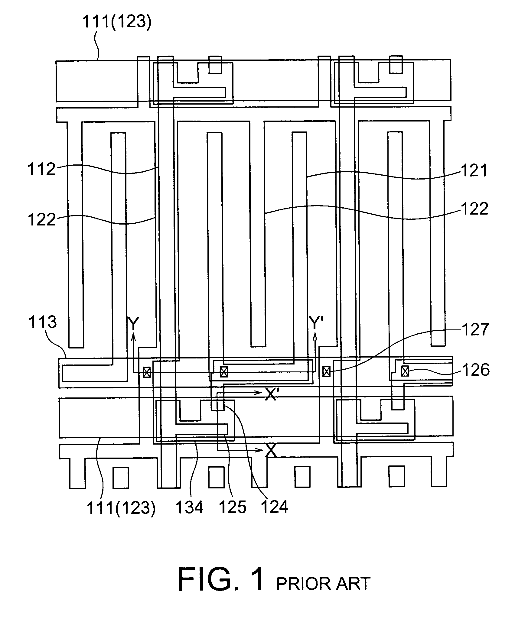
[0055]As shown in FIG. 4, on a surface of the TFT substrate 10 on its side facing an opposing substrate, scan lines 11 and signal lines 12 are provided so as to cross each other at right angles, and common lines 13 of common wiring are provided between the adjacent scan lines 11 in parallel therewith. In regions defined by crossing between the scan lines 11 and the signal lines 12, TFTs 14 are formed, respectively, so as to be arranged in a matrix. Scan line terminals 15 and signal line terminals 16 are provided at ends of the scan lines 11 and the signal lines 12, respectively, so as to receive drive signals from an external drive circuit.

[0056]The common lines 13 are mutually connected to form the common wiring for supplying a referential common potential for AC driving liquid crystals. Specifically, both ends of each common line 13 are connected to a pair of common-line connecting lines 17 which are arranged along short sides of the TFT substrate 10, respe...

Example

[0075](Second Embodiment)

[0076]In the second embodiment of the present invention, an interlayer insulating film on TFTs is formed only by an inorganic film. The structure of a TFT substrate is the same as that in the first embodiment shown in FIG. 4.

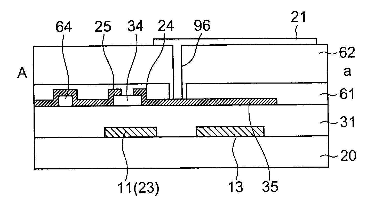
[0077]As shown in FIG. 22, in a region defined by crossing between scan lines 11 and signal lines 12 formed on the TFT substrate, a pixel electrode 21 and a common electrode 22 each formed like a comb having teeth are arranged with their teeth located alternately, and electric fields substantially parallel to the TFT substrate 10 are generated between the electrodes to thereby control orientation of liquid crystal molecules. As shown in FIGS. 23A to 23C, the pixel electrode 21 and the common electrode 22 are provided on an interlayer insulating film comprising two layers of passivation films 61 and 62 that are formed on a TFT 14.

[0078]Like in the first embodiment, the TFT 14 is an inverse stagger thin film transistor also in this embodim...

Example

[0086](Third Embodiment)

[0087]The third embodiment of the present invention, like the second embodiment, relates to a case wherein an interlayer insulating film on TFTs is formed only by an inorganic film. This embodiment only differs from the second embodiment in that the inorganic film of the interlayer insulating film is formed by a single layer, and the other structure thereof is the same as that of the second embodiment.

[0088]As shown in FIGS. 28A, 28B, and 28C, a pixel electrode 21 and a common electrode 22 are provided on an interlayer insulating film made of a single-layer passivation film 32 that is formed on a TFT 14.

[0089]Now, a manufacturing method of the TFT substrate according to the third embodiment will be described. What differs from the second embodiment only resides in passivation film forming and contact hole forming processes. Specifically, a passivation film 32 made of an inorganic film such as a silicon nitride film and having a thickness of about 700 to 1000 ...


PUM


Abstract

A display portion is divided by scan lines and signal lines into sections where pixels are provided. Contact holes each for connecting common wiring and a common electrode together are not formed for all the pixels, but decimated so as to be arranged in zigzags.

Description

[0001]This application claims priority to prior application JP 2002-268952, the disclosure of which is incorporated herein by reference.BACKGROUND OF THE INVENTION[0002]The present invention relates to a liquid crystal display and a method of manufacturing the same and, in particular, relates to an in-plane switching (IPS) liquid crystal display in which signal lines are partially covered with a common electrode via an interlayer insulating film.[0003]Conventionally, use has been widely made of transmission type liquid crystal displays employing thin film transistors (TFTs) or metal-insulator-metal (MIM) devices as switching elements for driving and controlling pixel electrodes. Particularly, IPS liquid crystal displays have been used as monitors, which can realize wide viewing angles like cathode ray tubes (CRTs).[0004]FIGS. 1 to 3 show structures of a one-pixel portion of an active matrix substrate in a conventional IPS liquid crystal display using TFTs disclosed in WO98 / 47044 (pp...

Claims


Application Information

Patent Timeline
IPC IPC(8): G02F1/1343G02F1/1333G02F1/1362G02F1/1368
CPCG02F1/134363G02F1/136227G02F1/133345
Inventor SAIGO, SHINGOHAYASE, TAKASUKEHORINOUCHI, MAKOTOMOTOSHIMA, HIDETOMAEDA, AKITOSHI
Owner NEC LCD TECH CORP
Why Eureka
Try Eureka