Techniques for mounting a circuit board component to a circuit board

Active Publication Date: 2006-08-01
EMC IP HLDG CO LLC
View PDF27 Cites 55 Cited by
  • Summary
  • Abstract
  • Description
  • Claims
  • Application Information

AI Technical Summary

Benefits of technology

[0016]In one arrangement, the set of soldering pads includes a first surface mount pad which is configured for copper-defined soldering and a second surface mount pad which is configured for mask-defined soldering. For example, the metallic material of the second surface mount pad can have a substantially rectangular or square shape, but the exposed surface of the pad can have a trapezoidal shape (e.g., a trapezoid shaped surface exposed by a transparent solder mask). This arrangement enables a circuit board manufacturer to easily distinguish the two pads visually, as well as standardize which pad is intended to connect to the anode of a diode component, and which pad is intended to connect to the cathode of the diode component. Accordingly, the manufacturer is not dependent on reading printed polarity ink markings which are often inconsistent, and difficult to read. Rather, with this arrangement of the invention, such a configuration (e.g., anodes always mount to the copper-defined pad) can be made into an industry-wide or company-wide standard thus permanent

Problems solved by technology

Unfortunately, there are deficiencies to the above-described conventional approaches to soldering small-sized circuit board components to circuit boards.
In some situations, the pulling force can be so great that a component terminal moves completely away from a pad resulting in an open circuit (i.e., an electrical discontinuity) between that terminal and the pad.
Furthermore, in both the pre-glued approach and the printed paste approach, the rectangular-shaped SMT pads (e.g., roughly 50 to 60 mils in width and length) to which the component contacts mount are often very large and require a substantial amount of circuit board surface “real estate”.
As a result, it can be diff

Method used


Image

  • Techniques for mounting a circuit board component to a circuit board
  • Techniques for mounting a circuit board component to a circuit board
  • Techniques for mounting a circuit board component to a circuit board

Examples


Example

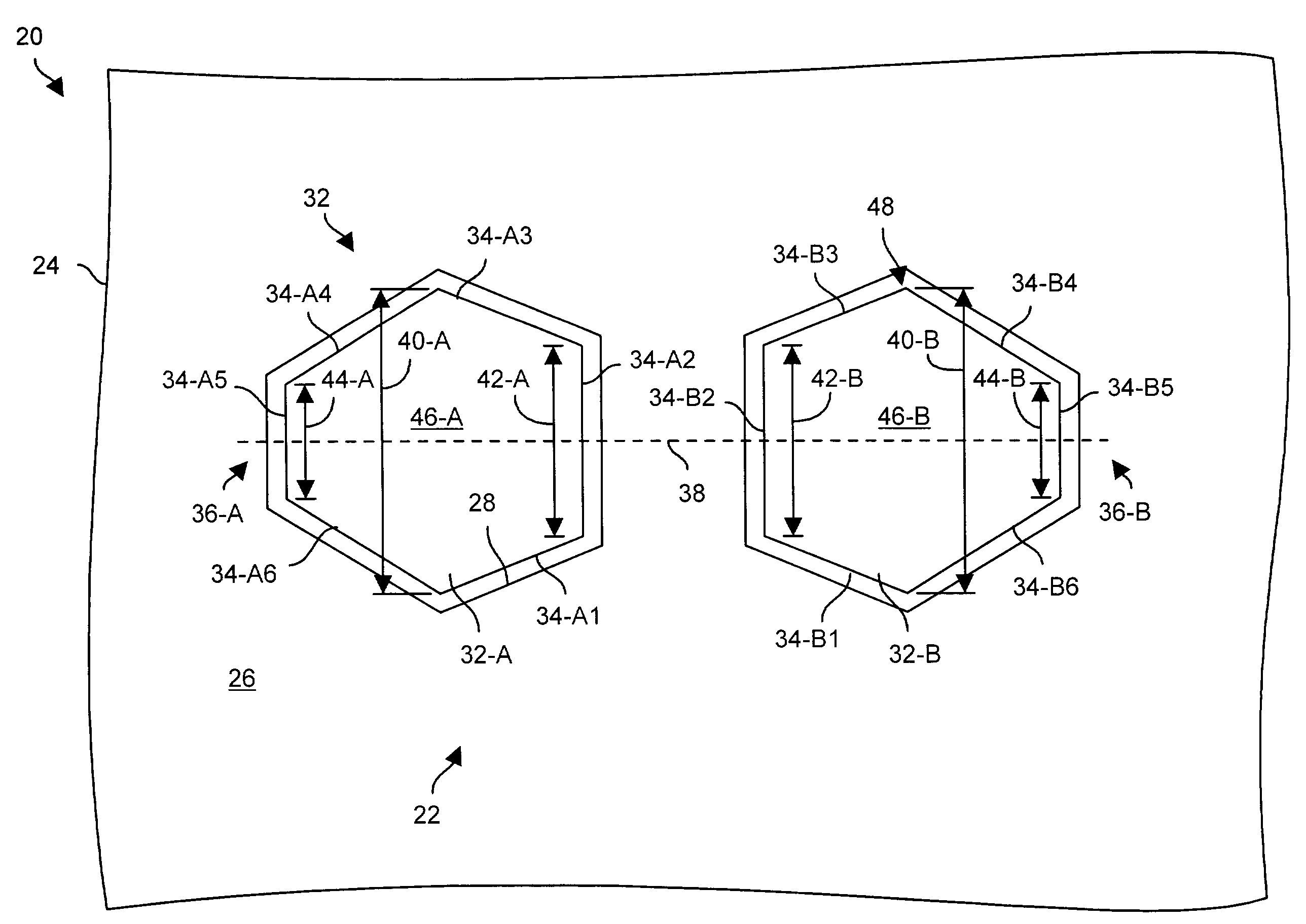
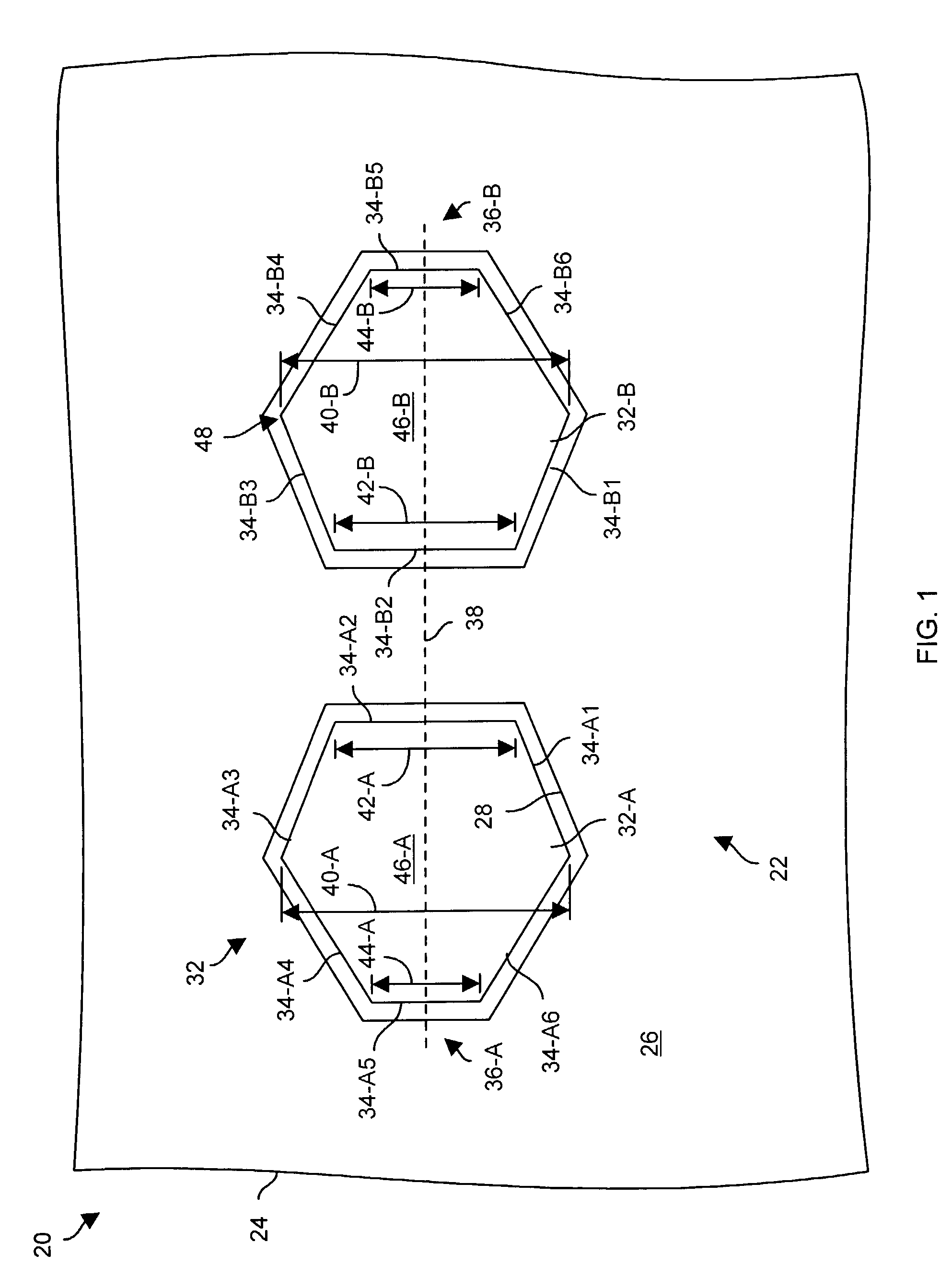
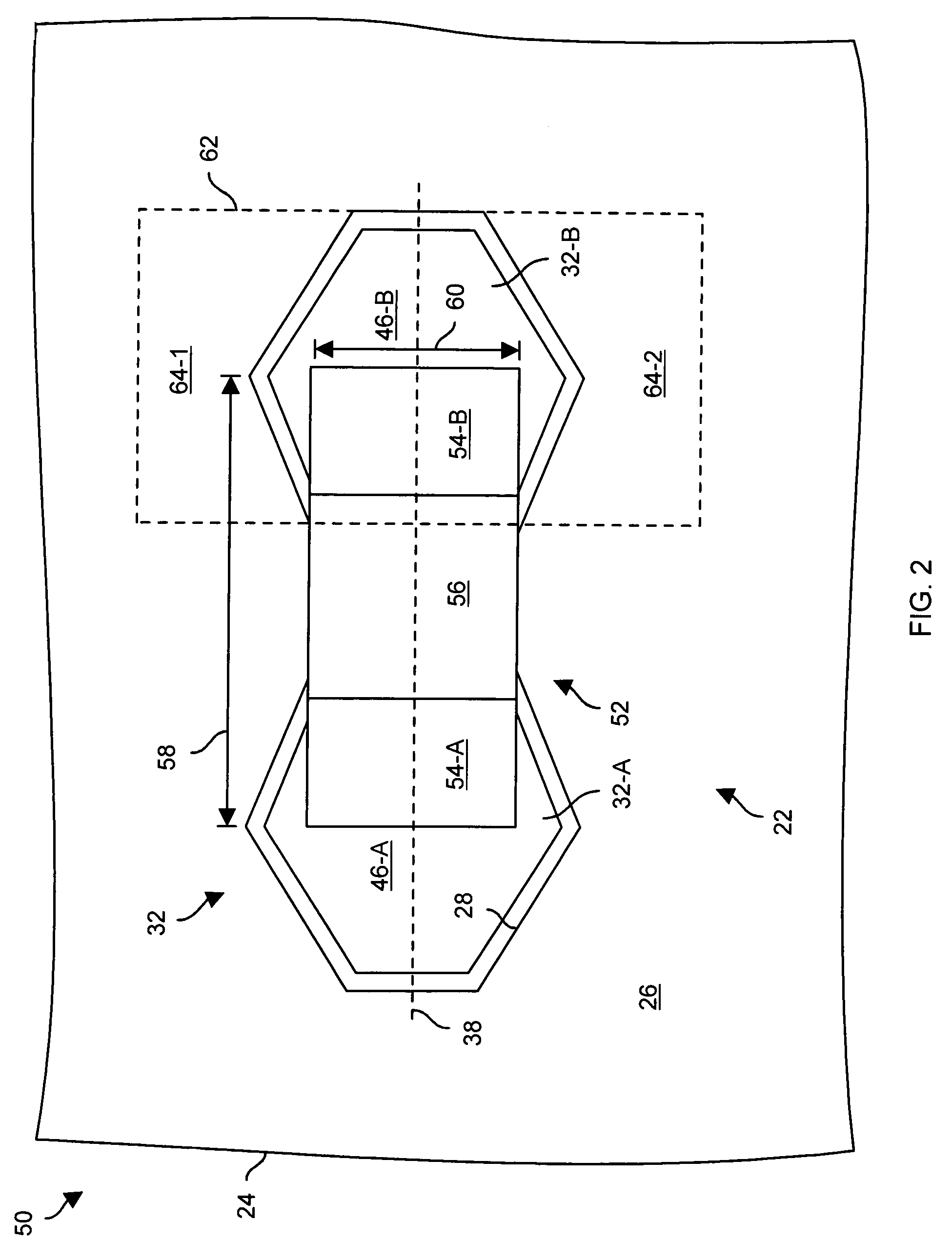
[0026]Embodiments of the invention are directed to techniques for mounting a circuit board component to a circuit board using generally trapezoid-shaped pads. The use of such pads (i) enables reliable mounting of circuit board components using a conventional soldering process such as printed paste soldering, as well as (ii) inhibits improper movement of the circuit board component if solder joints holding the component to the pads re-flow. Accordingly, the use of such techniques are well-suited for circuit board manufacturing processes which involve multiple heating phases (e.g., multiple passes through an oven resulting in re-melting of earlier-formed solder joints). Additionally, the use of such pads alleviates the need for alternative soldering solutions such as the use of high-temperature solder in an initial higher-temperature soldering process which could damage components due to higher temperature stresses. The techniques of the invention tend to raise circuit board manufactu...


PUM


Abstract

A circuit board has a layer of non-conductive material, and a set of soldering pads disposed on the layer of non-conductive material. The set of soldering pads defines a common axis that extends substantially through a midline of each soldering pad. Each soldering pad has, as measured perpendicularly through the common axis, an inner width, a first edge width and a second edge width. The inner width is longer than each of the first and second edge widths. Additionally, the first edge width is longer than the second edge width. Accordingly, the pads have less corner spaces that could otherwise, with melted solder, draw a circuit board component into an incorrect orientation which would result in incorrect mounting of the component. As a result, the component terminals tend to be drawn toward central regions of each pad for robust and reliable solder joint formation.

Description

BACKGROUND OF THE INVENTION[0001]A typical circuit board assembly includes a circuit board (i.e., layers of conductive and non-conductive material sandwiched together), and a variety of circuit board components which mount to the circuit board. Examples of circuit board components include, among other things, integrated circuits (ICs), individual circuit elements (e.g., resistors, capacitors, etc.), and connectors. Some components (e.g., lead frame packages, individual resistors, electrical connectors, etc) have leads which insert into and solder to sets of plated-through holes which extend through the circuit board. Other components (e.g., Ball Grid Array (BGA) packages, ceramic chips, etc.) solder to sets of surface mounting technology (SMT) pads or contacts disposed on the surface of the circuit board.[0002]Some components include relatively large-sized packages such as BGA packages which, in some instances, can be approximately two inches by two inches (or more) in area. Contact...

Claims


Application Information

Patent Timeline
IPC IPC(8): H01R12/04
CPCH05K1/111H05K3/3442H05K2203/048H05K2201/10636H05K2201/09381Y02P70/50
Inventor DOWNES, STUART D.
Owner EMC IP HLDG CO LLC
Why Eureka
Try Eureka