Liquid crystal display device

a display device and liquid crystal technology, applied in static indicating devices, non-linear optics, instruments, etc., can solve the problems of short life of backlight itself, high power consumption, and insufficient addition of sub-pixels to one pixel, so as to improve viewing angle, reduce suppress the effect of aperture ratio

Active Publication Date: 2013-12-31
SEMICON ENERGY LAB CO LTD
View PDF54 Cites 62 Cited by
  • Summary
  • Abstract
  • Description
  • Claims
  • Application Information

AI Technical Summary

Benefits of technology

[0006]Although a viewing angle characteristic can be improved by providing a sub-pixel in a pixel to make an oriented state different, only one additional sub-pixel to one pixel is inadequate. The viewing angle characteristic can be further improved by providing more sub-pixels; and as a result, image quality can be improved. On the other hand, as the number of sub-pixels increases, a decrease in an aperture ratio may be expected.
[0007]If the aperture ratio decreases, the luminance decreases. In order to suppress a decrease in the luminance, it is necessary to increase the luminance of a backlight. If the luminance of the backlight increases, power consumption becomes high. Alternatively, the life of the backlight itself becomes short. Alternatively, an increase in the temperature inversely affects liquid crystal materials and a color filter, and the life of a display device may be short. Alternatively, a decrease in the aperture ratio may make density of arrangement of wirings and electrodes high. As a result, a short-circuit of wirings or electrodes may occur by dust, remaining of etching, or the like. Accordingly, the manufacturing yield decreases. As the manufacturing yield decreases, cost becomes high.
[0008]In view of the aforementioned problems, it is an object of the present invention to provide a display device in which a viewing angle characteristic is improved by providing a plurality of sub-pixels in one pixel. Further, it is another object of the present invention to provide a display device in which a decrease in the aperture ratio is suppressed even when a plurality of sub-pixels is provided. Furthermore, it is another object of the present invention to provide a display device in which a decrease in the luminance is suppressed. Furthermore, it is another object of the present invention to provide a display device in which power consumption is suppressed. Furthermore, it is another object of the present invention to provide a display device in which a shortening of the life is suppressed. Furthermore, it is another object of the present invention to provide a display device in which thermal elevation is suppressed. Furthermore, it is another object of the present invention to provide a display device in which a manufacturing yield is improved. Furthermore, it is another object of the present invention to provide a display device in which a cost is cut. Furthermore, it is another object of the present invention to provide a display device in which image quality is improved.

Problems solved by technology

Although a viewing angle characteristic can be improved by providing a sub-pixel in a pixel to make an oriented state different, only one additional sub-pixel to one pixel is inadequate.
If the luminance of the backlight increases, power consumption becomes high.
Alternatively, the life of the backlight itself becomes short.
Alternatively, an increase in the temperature inversely affects liquid crystal materials and a color filter, and the life of a display device may be short.
As a result, a short-circuit of wirings or electrodes may occur by dust, remaining of etching, or the like.
As the manufacturing yield decreases, cost becomes high.

Method used


Image

  • Liquid crystal display device
  • Liquid crystal display device
  • Liquid crystal display device

Examples


embodiment mode 1

[0169]In this embodiment mode, a structural example of a display device of the present invention will be described with reference to drawings.

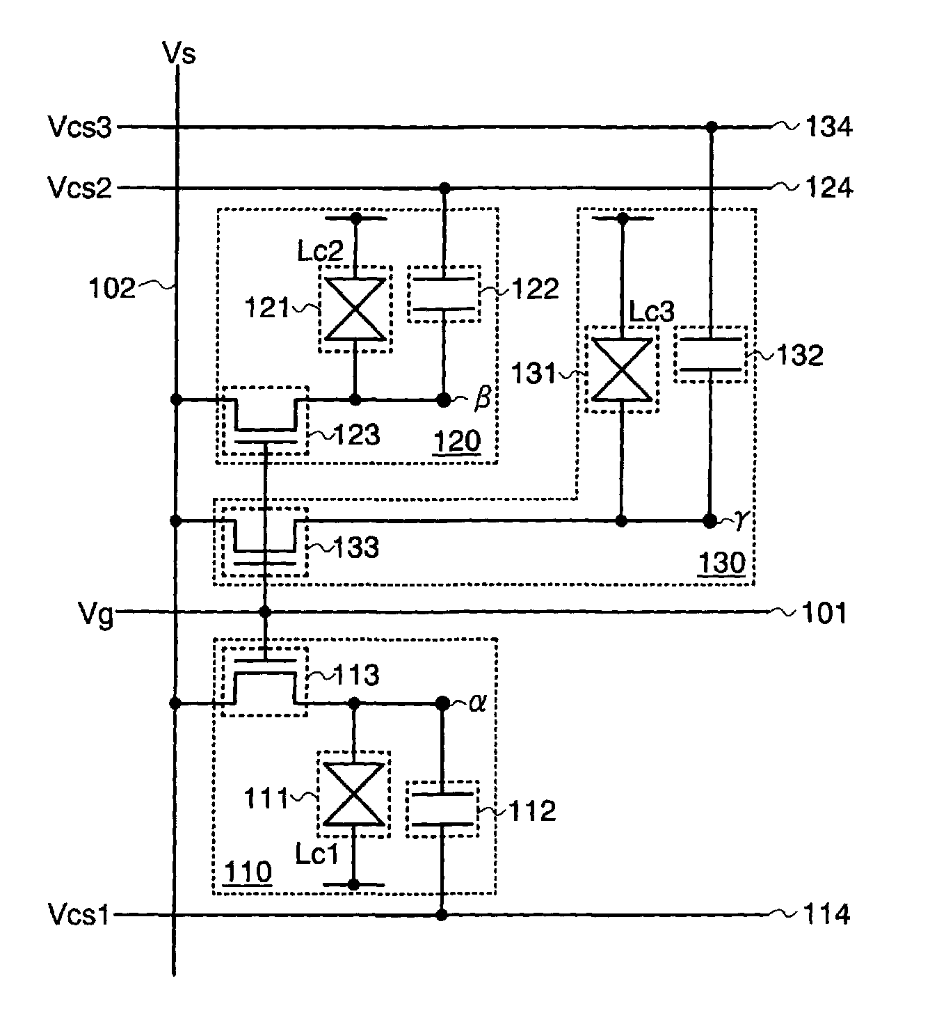
[0170]A display device described in this embodiment mode includes a plurality of pixels and a plurality of sub-pixels is provided for each of the pixels. A structure of one pixel will be described with reference to FIG. 1.

[0171]FIG. 1 shows a structure of a pixel which is provided with three sub-pixels. A first sub-pixel 110 includes a first liquid crystal layer 111, a first capacitor element 112, and a first transistor 113. Similarly, a second sub-pixel 120 includes a second liquid crystal layer 121, a second capacitor element 122, and a second transistor 123; and a third sub-pixel 130 includes a third liquid crystal layer 131, a third capacitor element 132, and a third transistor 133. Although a structure provided with transistors is shown here, other switching elements such as a diode may be provided.

[0172]Each of the first liquid crystal l...

embodiment mode 2

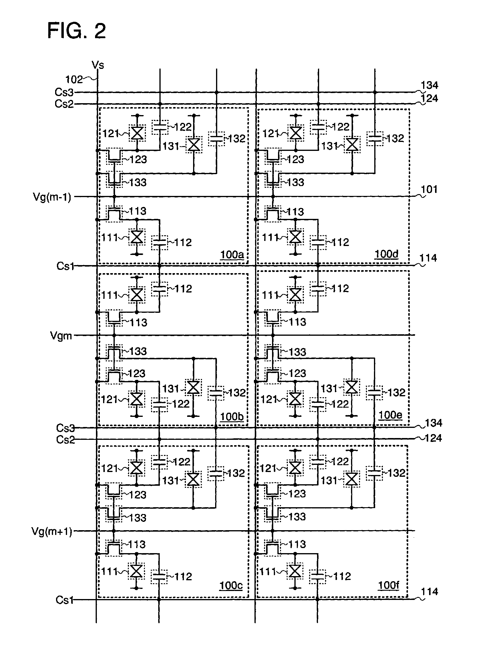
[0232]In this embodiment mode, a structure of a display device, which is different from that shown in Embodiment Mode 1, will be described with reference to diagrams. Specifically, with respect to the structure shown in Embodiment Mode 1, the case where the scanning line and the third capacitor wiring are provided as one is shown.

[0233]FIG. 4 shows a structure of pixels in a display device which is described in this embodiment mode. Note that FIG. 4 shows the structure in which three sub-pixels are provided in each of a plurality of pixels 100a to 100f. Specifically, the first sub-pixel is provided with the first liquid crystal layer 111, the first capacitor element 112, and the first transistor 113; the second sub-pixel is provided with the second liquid crystal layer 121, the second capacitor element 122, and the second transistor 123; and the third sub-pixel is provided with the third liquid crystal layer 131, the third capacitor element 132, and the third transistor 133.

[0234]In...

embodiment mode 3

[0255]In this embodiment mode, a semiconductor device which is different from the above-described embodiment modes will be described with reference to diagrams.

[0256]FIG. 8 shows a structure of a pixel in a display device which will be described in this embodiment mode.

[0257]A pixel shown in FIG. 8 has a structure in which five sub-pixels are provided. The first sub-pixel 110 includes the first liquid crystal layer 111, the first capacitor element 112, and the first transistor 113. Similarly, the second sub-pixel 120 includes the second liquid crystal layer 121, the second capacitor element 122, and the second transistor 123; the third sub-pixel includes the third liquid crystal layer 131, the third capacitor element 132, and the third transistor 133; the fourth sub-pixel 140 includes the fourth liquid crystal layer 141, the fourth capacitor element 142, and the fourth transistor 143; and a fifth sub-pixel 150 includes a fifth liquid crystal layer 151, a fifth capacitor element 152,...


PUM

PropertyMeasurementUnit
semiconductoraaaaaaaaaa

Abstract

To provide a display device in which a viewing angle characteristic is improved by providing a plurality of sub-pixels to one pixel. Alternatively, to provide a display device in which an aperture ratio is suppressed even when a plurality of sub-pixels is provided. A pixel including first sub-pixel, a second sub-pixel, and a third sub-pixel, a scanning line, a signal line, a first capacitor wiring, a second capacitor wiring and a third capacitor wiring are provided. Pixel electrodes each electrically connected to one electrode of the first to third capacitor elements, and the first to third capacitor wirings, respectively, are provided to the first to third sub-pixels electrodes, respectively. Potentials of the first capacitor wiring and the second capacitor wiring are changed and a potential of the third capacitor wiring is kept almost constant.

Description

BACKGROUND OF THE INVENTION[0001]1. Field of the Invention[0002]The present invention relates to an object, a method or a manufacturing method of an object. Specifically, the present invention relates to a display device or a semiconductor device. More specifically, the present invention relates to a display device provided with a plurality of sub-pixels in a pixel.[0003]2. Description of the Related Art[0004]Recently, low-profile display devices including a liquid crystal display device have been widely used for displays of cell phones, televisions, and the like. In particular, liquid crystal display devices have excellent features such as high resolution, low profile, and low power consumption and the market size is being expanded. On the other hand, more and more improvement of performance is required for these display devices. For example, a wide viewing angle and high image quality are required for a liquid crystal display device.[0005]As a technique for improving a viewing ang...

Claims


Application Information

Patent Timeline
Patent Type & Authority Patents(United States)
IPC IPC(8): G09G3/36G02F1/1343
CPCG02F1/13624G09G2310/0251G09G3/342G09G2300/0443G09G2320/028G09G2320/0261G02F2001/134345G09G3/3659G09G2300/0426G09G2340/16G09G2320/0252G09G3/2025G09G2310/024G09G2320/0673G09G3/3607G09G2340/0435G09G2320/0276G09G3/3655G09G2300/0465G02F1/134345
Inventor KIMURA, HAJIME
Owner SEMICON ENERGY LAB CO LTD
Why Eureka
Try Eureka