Semiconductor-device manufacturing method

a manufacturing method and semiconductor technology, applied in semiconductor devices, semiconductor/solid-state device details, electrical devices, etc., can solve the problems of high accuracy of the outside dimensions of the semiconductor chip, inadequacies of methods, and thin blade width, so as to facilitate the production of semiconductor chips and prevent the scattering of semiconductor substrate materials during the dicing process. , the effect of high accuracy of the outside dimensions

Inactive Publication Date: 2006-10-05
FUJITSU SEMICON LTD
View PDF6 Cites 63 Cited by
  • Summary
  • Abstract
  • Description
  • Claims
  • Application Information

AI Technical Summary

Benefits of technology

[0029] According to the semiconductor-device manufacturing method of the present invention, it is possible to easily produce the semiconductor chips with high accuracy of the outside dimensions. And the scattering of the semiconductor substrate materials when the dicing pr

Problems solved by technology

This method is not appropriate for the case where high accuracy of the outside dimensions of the semiconductor chip is required.
However, in the above-mentioned method, the blade width becomes thin due to wearing of the blade produced every time the dicing action is performed at a time, and the accuracy of the outside dimensions becomes insufficient.
This method is also inappropria

Method used


Image

  • Semiconductor-device manufacturing method
  • Semiconductor-device manufacturing method
  • Semiconductor-device manufacturing method

Examples


Embodiment Construction

[0038] A description will now be given of the preferred embodiments of the present invention with reference to the accompanying drawings.

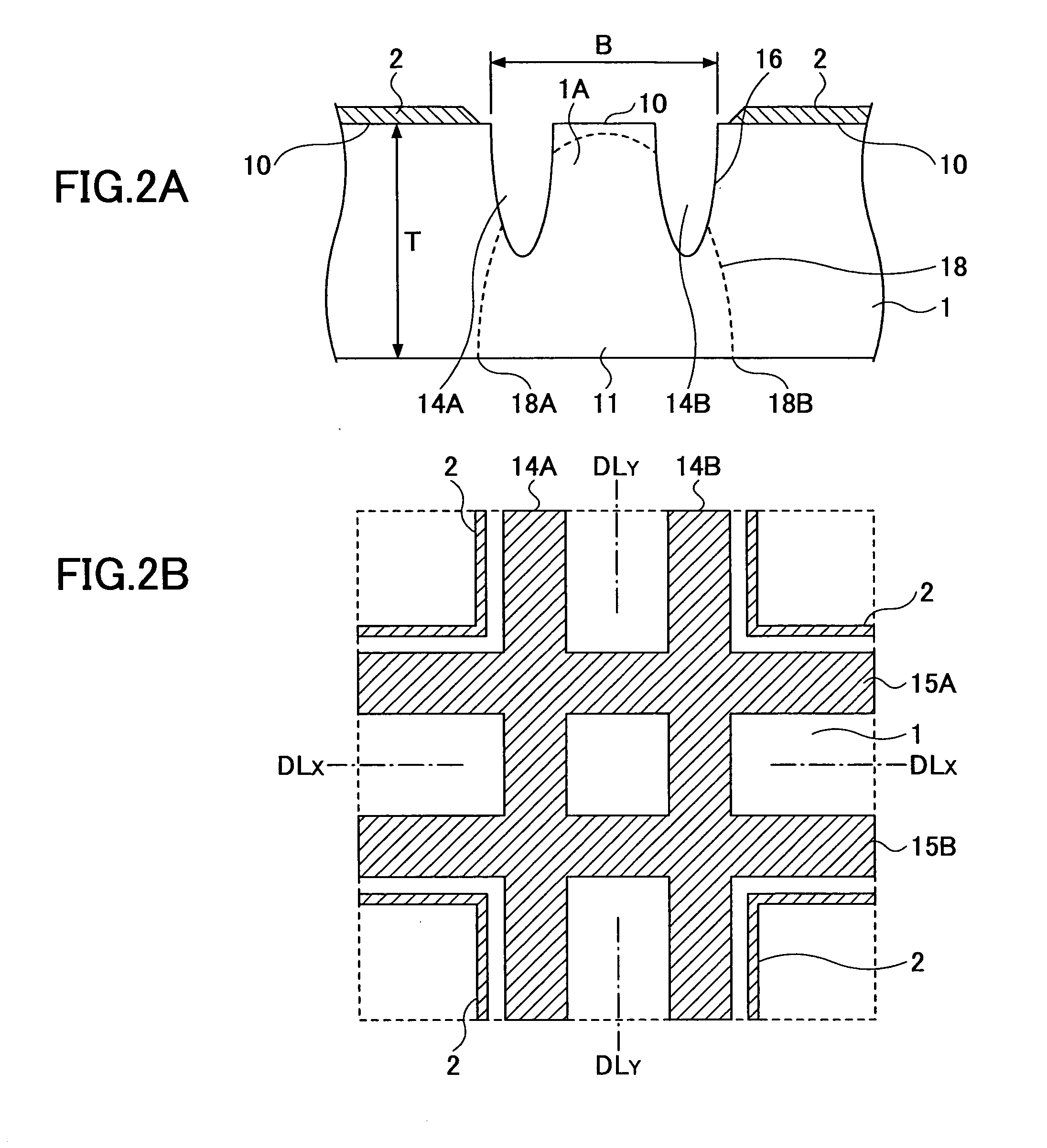
[0039]FIG. 2A and FIG. 2B show the structure of the dicing grooves in the semiconductor substrate which are formed according to the semiconductor-device manufacturing method in one embodiment of the invention.

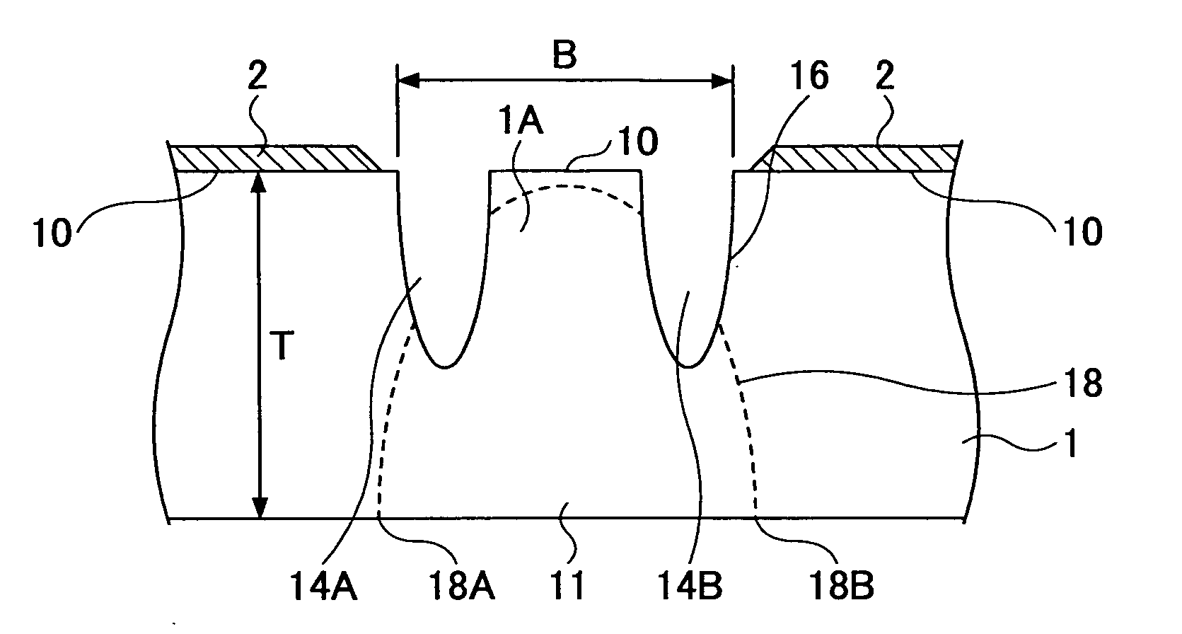
[0040] In FIG. 2A and FIG. 2B, the reference numeral 1 denotes the semiconductor substrate (wafer), 2 denotes the metal layer which is arranged at the outermost periphery of each of the plurality of semiconductor chips arranged in the matrix formation on one of the principal surfaces (the front surface 10) of the substrate 1 concerned and forms the moisture-resistant ring.

[0041] Moreover, in FIG. 2A and FIG. 2B, the reference numeral 11 denotes the other of the principal surfaces (the back surface) of the substrate 1 concerned, 14A, 14B, 15A, 15B denote the dicing grooves which are formed along the dicing lines DLx and DLy in the lengthwise...


PUM


Abstract

In a manufacturing method of a semiconductor device, a semiconductor substrate having a plurality of semiconductor chips formed on one of principal surfaces of the substrate is cut into the plurality of semiconductor chips through dicing. A first cutting process is formed on one of the principal surfaces of the substrate to produce two cutting grooves between two neighboring ones of the plurality of semiconductor chips, each cutting groove being adjacent to one of the neighboring ones of the plurality of semiconductor chips. A second cutting process is performed on the other of the principal surfaces of the substrate to produce a cutting groove overlapping the two cutting grooves produced by the first cutting process.

Description

CROSS-REFERENCE TO RELATED APPLICATIONS [0001] This application is based upon and claims the benefit of priority of Japanese Patent Application No. 2005-105233, filed on Mar. 31, 2005, the entire contents of which are herein incorporated by reference. BACKGROUND OF THE INVENTION [0002] 1. Field of the Invention [0003] The present invention relates to a manufacturing method of a semiconductor device in which a semiconductor substrate (wafer) having a plurality of semiconductor chips formed on one of principal surfaces of the substrate is cut into the semiconductor chips through dicing. [0004] 2. Description of the Related Art [0005] In electronic devices, such as a sensor chip, in which the plurality of semiconductor devices are adjoined to each other and mounted as the module, it is necessary to shorten the distance between the adjacent semiconductor devices as much as possible, and make the sensor region continuous without interruption. What is required for such electronic devices ...

Claims


Application Information

Patent Timeline
IPC IPC(8): H01L21/00
CPCH01L21/6836H01L21/78H01L23/585H01L2221/68327H01L2924/0002H01L2924/00H01L21/30
Inventor TERAYAMA, SATOSHIMATSUKI, HIROHISA
Owner FUJITSU SEMICON LTD
Why Eureka
Try Eureka