Flat panel display and method of manufacturing the same

Inactive Publication Date: 2005-05-19
NORITAKE CO LTD
View PDF1 Cites 10 Cited by
  • Summary
  • Abstract
  • Description
  • Claims
  • Application Information

AI Technical Summary

Benefits of technology

[0015] It is an object of the present invention to pro

Problems solved by technology

The conventional flat panel display, however, has the following problems.
Also, as the voltage to be applied to the gate electrode is high, the power consumption also increases.
Accordingly, during alignment, the surface of the electron-emitting source rubs against the lower surface of the gate electrode surface, and is acco

Method used


Image

  • Flat panel display and method of manufacturing the same
  • Flat panel display and method of manufacturing the same
  • Flat panel display and method of manufacturing the same

Examples


Example

First Embodiment

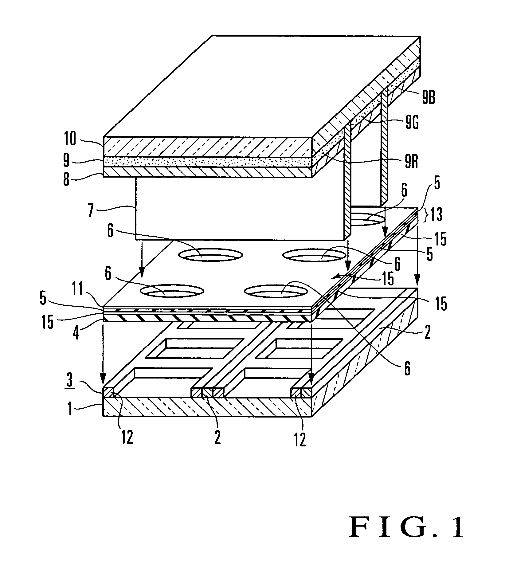
[0049] As shown in FIG. 1, a flat panel display according to the first embodiment has a vacuum envelope with a front glass plate 10 which is at least partly transparent and a glass substrate 1 opposing the front glass plate 10 and having a substantially rectangular shape when seen from the top, and a cathode 3 formed on the glass substrate 1 and having electron-emitting sources in its predetermined region.

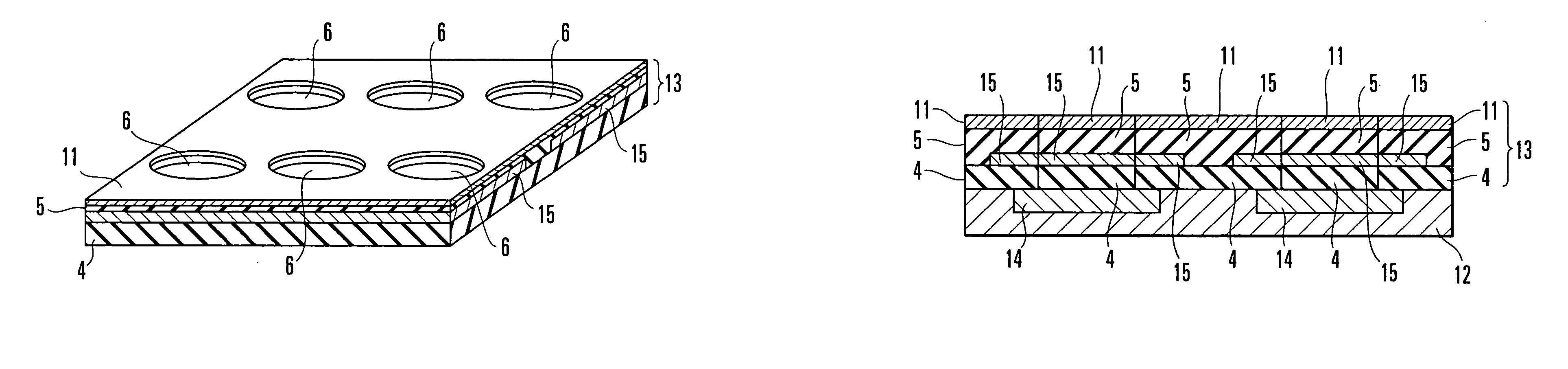
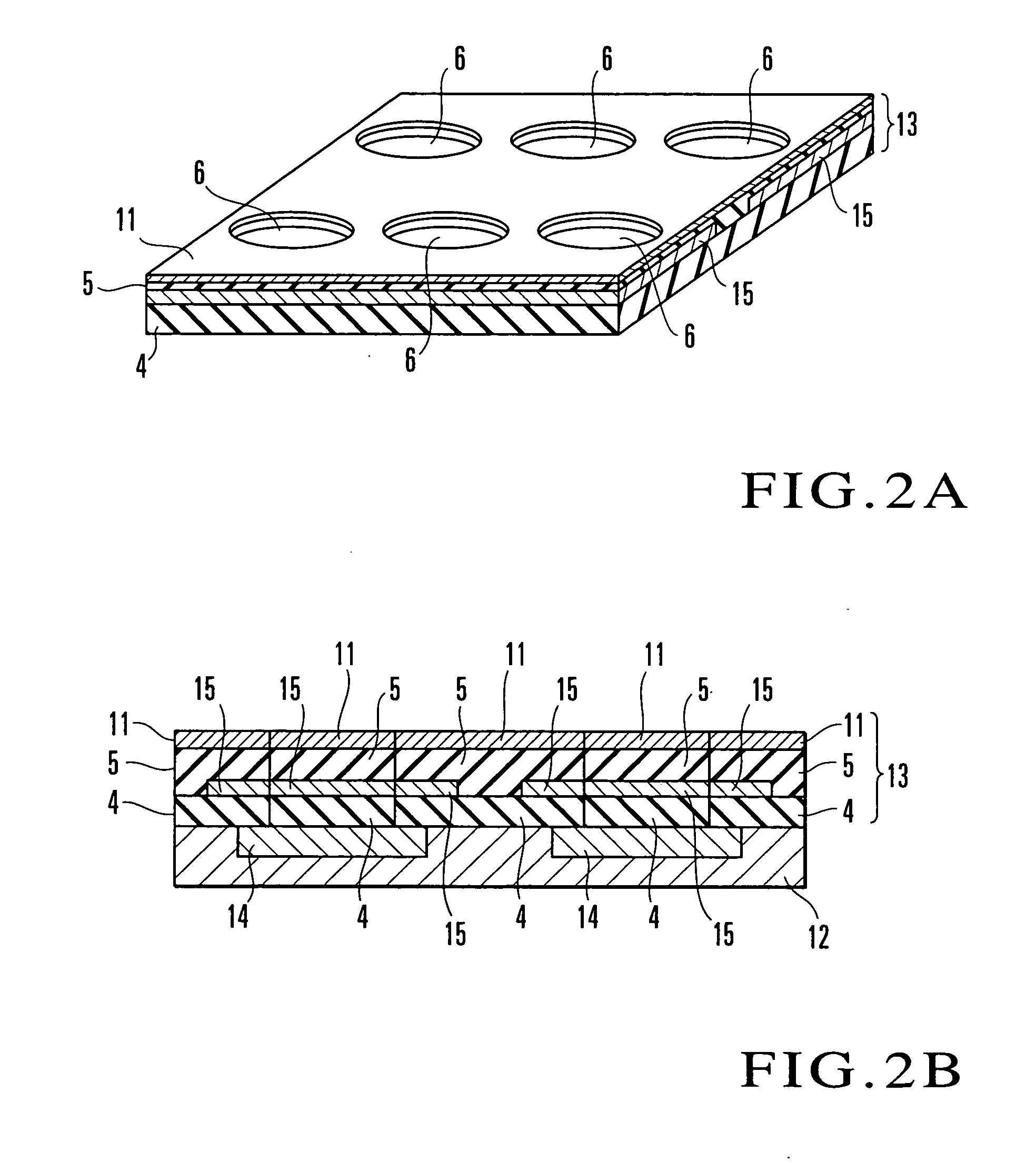
[0050] The flat panel display also has a gate electrode substrate 13 having electron-passing holes 6 and arranged in the envelope to oppose the glass substrate 1 to be separate from the cathode 3, and a phosphor screen 9 and anode electrode 8 which are formed on the surface of the front glass plate 10 in the vacuum envelope.

[0051] The cathode 3 has a plurality of band-like cathodes 12 which are arranged parallel to each other. The band-like cathodes 12 form electron-emitting sources 14. Substrate ribs 2 are arranged between the plurality of band-like cathodes 12....

Example

Second Embodiment

[0133] The second embodiment will be described with reference to the accompanying drawings.

[0134] A flat panel display according to the second embodiment is a flat panel display in which the structures of the gate electrode substrate and cathode are improved to improve the display uniformity. The flat panel display according to the second embodiment is constituted by a substrate, gate electrode substrates 11, front ribs 7, and a panel plate, as shown in FIG. 8.

[0135] The substrate will be described. The substrate is formed of a glass substrate 1 having a substantially rectangular shape when seen from the top, substrate ribs 2, and a cathode 3.

[0136] The cathode 3 is formed of cathode substrates 12 and electron-emitting sources 14. Each cathode substrate 12 is obtained by machining a substrate having a conductive surface, e.g., a metal member made of a 426-alloy and having a thickness of about 0.1 mm to 0.15 mm, into a band-like shape. Furthermore, as shown in FI...


PUM


Abstract

A flat panel display includes a vacuum envelope, a cathode, a gate electrode substrate, and a phosphor screen and anode electrode. The vacuum envelope includes a front glass plate which is at least partly transparent and a substrate opposing the front glass plate. The cathode is formed on the substrate and has an electron-emitting source. The gate electrode substrate has an electron-passing hole and is arranged in the vacuum envelope to oppose the substrate to be separate from the cathode. The phosphor screen and anode electrode are formed on a surface of the front glass plate in the vacuum envelope. The gate electrode substrate includes at least an insulating substrate and a gate electrode. The insulating substrate has the electron-passing hole. The gate electrode is formed on the insulating substrate. A method of manufacturing a flat panel display is also disclosed.

Description

BACKGROUND OF THE INVENTION [0001] The present invention relates to a flat panel display which emits light by causing electrons emitted from an electron-emitting source to bombard on a phosphor screen and, more particularly, to a flat panel display which uses nanotube fibers as an electron-emitting source. [0002] In recent years, a flat panel display such as a field emission display (FED) or a field emission display which uses nanotube fibers, e.g., carbon nanotubes, as the electron-emitting source of a flat vacuum fluorescent display has been proposed and attracts attention. [0003] A carbon nanotube is a material with a structure in which a single graphite layer is cylindrically closed and a five-membered ring is formed at the distal end of the cylinder. As the carbon nanotube is chemically stable, it is not easily influenced by a residual gas. The typical diameter of the carbon nanotube is as very small as 10 nm to 50 nm to provide a material having a high aspect ratio. Hence, the...

Claims


Application Information

Patent Timeline
IPC IPC(8): H01J29/46H01J29/48H01J31/00H01J31/12
CPCB82Y10/00H01J29/467H01J2201/30469H01J31/127H01J29/481H01J1/30B82Y40/00
Inventor YOTANI, JUNKOUEMURA, SASHIRO
Owner NORITAKE CO LTD
Why Eureka
Try Eureka