Particle movement-type display device and particle movement-type display apparatus

a display device and particle movement technology, applied in static indicating devices, instruments, optics, etc., can solve the problems of adverse affect of display state and inability to achieve uniform black display, and achieve bright and uniform display

Inactive Publication Date: 2006-06-08
CANON KK
View PDF11 Cites 22 Cited by
  • Summary
  • Abstract
  • Description
  • Claims
  • Application Information

AI Technical Summary

Benefits of technology

[0009] An object of the present invention is to provide an electrophoretic display device, as an example of a particle movement type display device, capable of effecting bright and uniform display.
[0018] In the particle movement type display device, the first electrode is formed at a part of a portion, corresponding to the pixel, on the first substrate on an observer side and a non-electrode forming portion where the first electrode is not formed is provided at another part of the portion on the first substrate. As a result, it becomes possible to effect bright and uniform display.

Problems solved by technology

However, there is a possibility that a display state is adversely affected when a strange electric charge is externally exerted on the surface of the front-side substrate, so that an electrode may preferably be disposed also on the surface of the front-side substrate in some cases in order to prevent the above-described phenomenon.
As a result, uniform black display cannot be effected.

Method used


Image

  • Particle movement-type display device and particle movement-type display apparatus
  • Particle movement-type display device and particle movement-type display apparatus
  • Particle movement-type display device and particle movement-type display apparatus

Examples


example 1

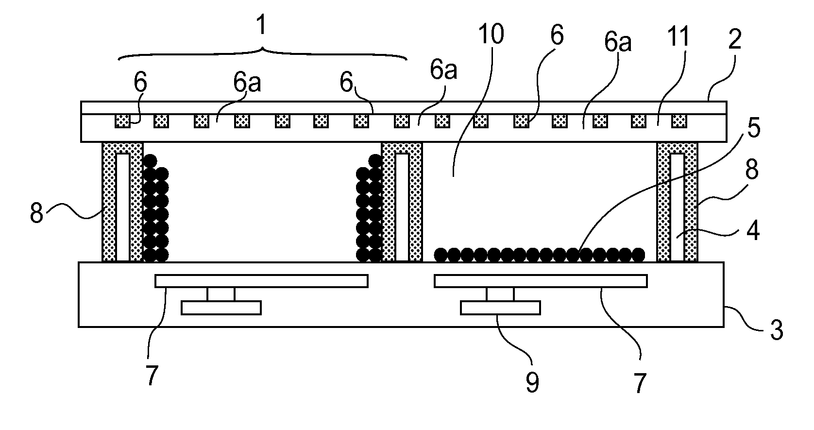
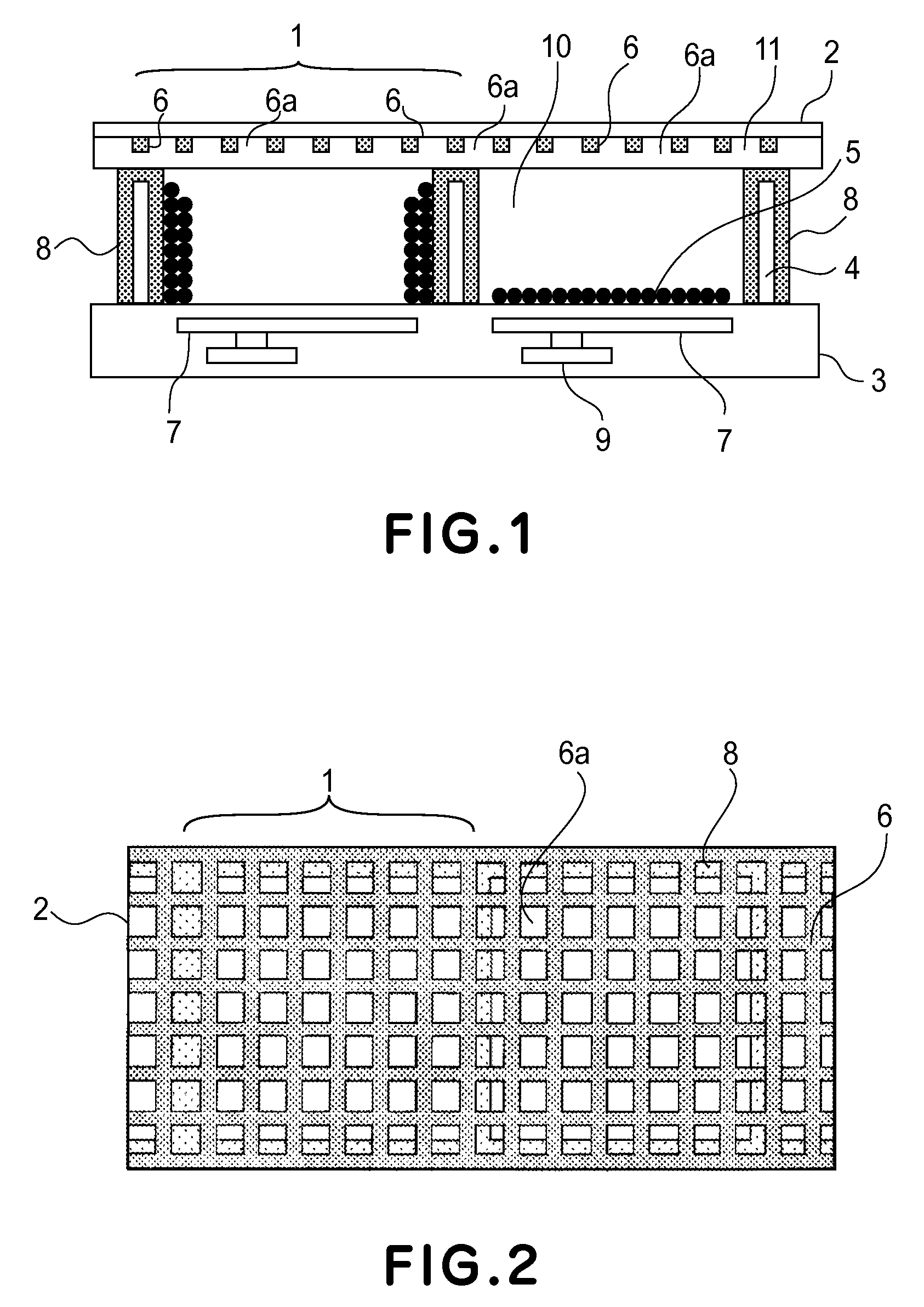
[0055] In this example, an electrophoretic display device having a structure shown in FIG. 1 was prepared in the following manner.

[0056] On a second substrate 3 formed of glass, TFT9 and wires were formed and thereon a second electrode 7 was disposed pixel by pixel through an insulating layer. The second electrode 7 was formed of aluminum and had a surface provided with a minute unevenness so as to perform reflection and scattering of incident light. Thereafter, a partition wall 4 was disposed through an insulating layer at a boundary of adjacent pixels and then a black third electrode 8 was formed at the surface of the partition wall 4. Thereafter, the third electrode 8 was coated with an insulating layer.

[0057] Next, in a space defined by the second substrate 3 and the partition wall 4, a transparent insulating liquid 10 in which charged particles 5 were dispersed was filled and thereon a first substrate 2 having a lattice-like ITO transparent electroconductive layer as a first ...

example 2

[0059] In this example, an electrophoretic display device was prepared in the same manner as in Example 1 except that a lattice-like ITO transparent electrode layer as a first electrode 6 was formed on the surface of the first substrate 2 and was covered with a transparent resin layer 11 having a volume resistivity of about 1.0×10⁷ ohm.cm at the entire electrode surface. An electrode forming areal ratio per a pixel area of pixel was 40%.

[0060] Then, in an electrophoretic display apparatus including the thus prepared electrophoretic display device, display was effected by applying predetermined voltages to the first electrode 6, the second electrode 7, and the third electrode 8, respectively, to drive the charged particles 5. As a result, according to this example, by setting the areal ratio of the transparent electrode layer as the first electrode 6 to a pixel area of each pixel to 40%, it is possible to suppress light absorption compared with the case of forming the transparent el...

example 3

[0061] In this example, an electrophoretic display device having a structure shown in FIG. 5(b) was prepared in the following manner.

[0062] On a second substrate 3 formed of glass, TFT9 and wires were formed and thereon a second electrode 7 formed of aluminum was disposed pixel by pixel through an insulating layer.

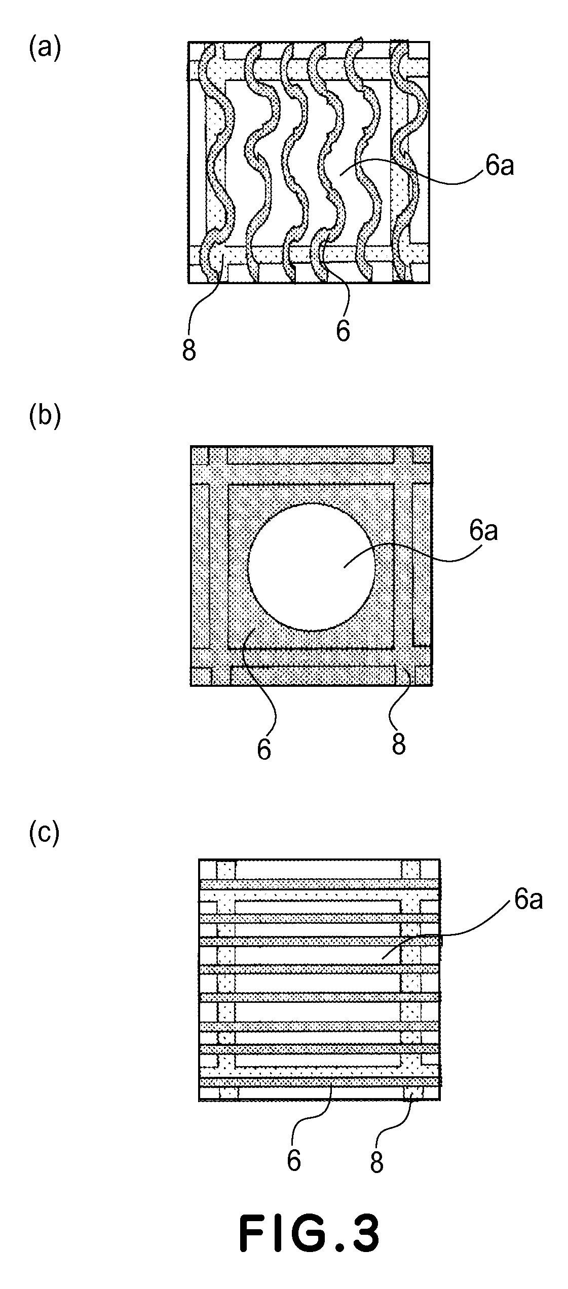
[0063] Next, on the second electrode 7, microcapsules 12 each comprising black charged particles 5a, white charged particles 5b, and an insulating liquid 10 were dispersed. On the surface thereon a first substrate 2 having an ITO transparent electroconductive layer as a first electrode 6 having a shape as shown in FIG. 4(a) was disposed. An electrode forming areal ratio per a pixel area of pixel was 50%.

[0064] Then, in an electrophoretic display apparatus including the thus prepared electrophoretic display device, display was effected by applying predetermined voltages to the first electrode 6, and the second electrode 7, respectively, to drive the charged particles 5. ...


PUM


Abstract

A particle movement type display device includes a plurality of pixels each of which is constituted by a first substrate and a second substrate disposed opposite to each other with a spacing therebetween, charged particles disposed between the first substrate and the second substrate, a first electrode and a second electrode disposed in contact with the spacing. An image is displayed by moving the charged particles under application of an electric field between the first electrode and the second electrode. The first electrode is formed on the first substrate at a part of a portion corresponding to each pixel and a non-electrode forming portion at which the first electrode is not formed is provided on the first substrate.

Description

FIELD OF THE INVENTION AND RELATED ART [0001] The present invention relates to a particle movement-type display device and a particle movement-type display apparatus, particularly a constitution of an electrode formed on a front-side (display-side) substrate. [0002] In recent years, study on reflection-type display apparatuses using no backlight has been actively made. Of these reflection-type display apparatuses, a particle movement-type display apparatus for effecting display by moving particles under application of voltage has received considerable attention. [0003] As an example of the particle movement-type display apparatus, an electrophoretic display apparatus is used. The electrophoretic display apparatus includes an electrophoretic display device constituted by a pair of substrates disposed opposite to each other with a predetermined spacing therebetween, charged particles (electrophoretic particles) disposed between the substrates, and a pair of electrodes disposed to face...

Claims


Application Information

Patent Timeline
Patent Type & Authority Applications(United States)
IPC IPC(8): G09G3/34
CPCG09G3/3446G09G2300/0439G09G2320/0233
Inventor IKEDA, TSUTOMU
Owner CANON KK
Why Eureka
Try Eureka