Amoled pixel driving circuit and pixel driving method

Active Publication Date: 2019-01-10
SHENZHEN CHINA STAR OPTOELECTRONICS SEMICON DISPLAY TECH CO LTD
View PDF0 Cites 2 Cited by
  • Summary
  • Abstract
  • Description
  • Claims
  • Application Information

AI Technical Summary

Benefits of technology

The present invention provides an improved pixel driving circuit and method for active-matrix organic light-emitting diodes (AMOLEDs) that overcomes the issues of threshold voltage and aging. This results in increased displaying uniformity and luminance of the panel, as well as higher luminous efficiency.

Problems solved by technology

Even if a same data voltage is applied to the driving thin film transistor of each pixel driving circuit, the current flowing through an organic light emitting diode of each pixel driving circuit still may not be the same, thereby affecting uniformity of image displaying quality.
Furthermore, as driving time of a driving thin film transistor becomes longer, aging and variation of material of the driving thin film transistor may appear, causing a threshold voltage of the driving thin film transistor to drift.
Further, a degree of aging of material of each driving thin film transistor may be different, and a drift amount of a threshold voltage of each driving thin film transistor may also be different, causing the panel to display non-uniformly.
Also, aging and variation of the material of the driving thin film transistor may cause a turn on voltage of the driving thin film transistor to increase, and a current flowing through an organic light emitting diode to decrease, resulting in problems such as decreased luminance and lowered luminous efficiency of the panel.

Method used


Image

  • Amoled pixel driving circuit and pixel driving method
  • Amoled pixel driving circuit and pixel driving method
  • Amoled pixel driving circuit and pixel driving method

Examples


Embodiment Construction

[0069]The description of each embodiment below refers to respective accompanying drawing(s), so as to illustrate exemplarily specific embodiments of the present disclosure that may be practiced. Directional terms mentioned in the present disclosure, such as “upper”, “lower”, “front”, “back”, “left”, “right”, “inner”, “outer”, “side”, etc., are only directions by referring to the accompanying drawings, and thus the used directional terms are used to describe and understand the present disclosure, but the present disclosure is not limited thereto. In the drawings, structurally similar units are labeled by the same reference numerals.

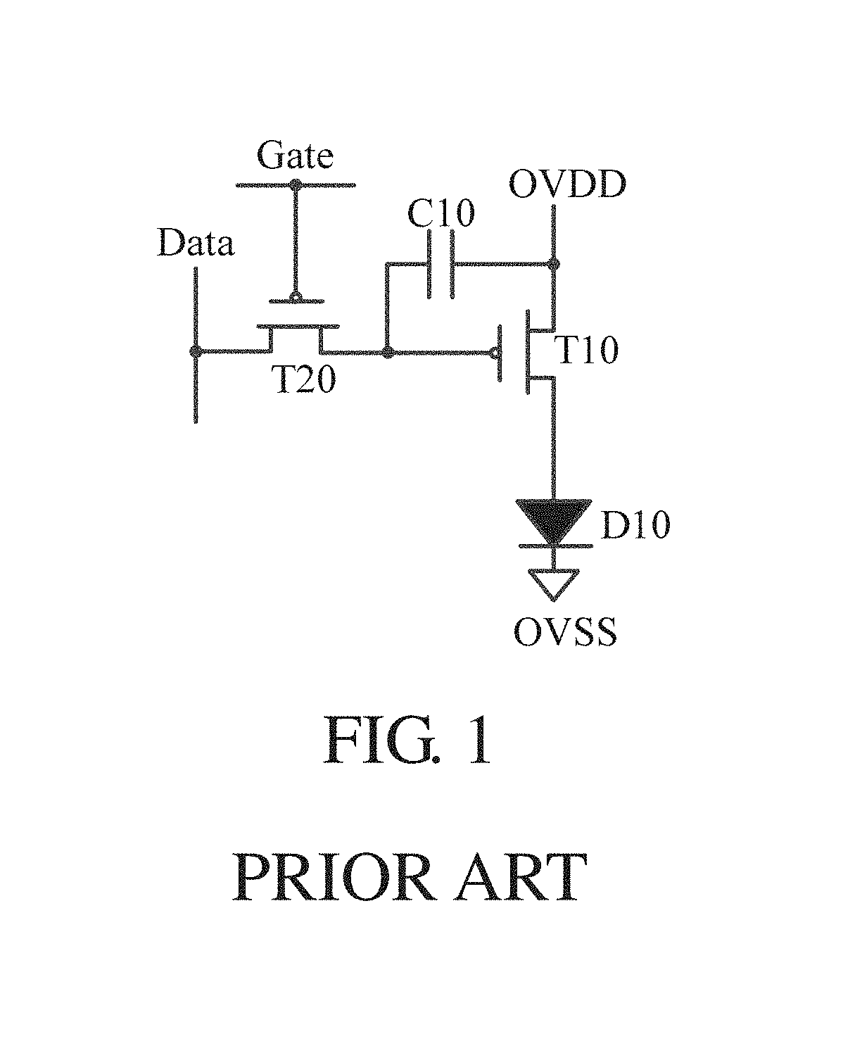
[0070]With respect to drifting problems for threshold voltages of driving thin film transistors, the prior art usually increases numbers of thin film transistors and corresponding control signals of active-matrix organic light-emitting diode (AMOLED) pixel driving circuits, to compensate the threshold voltages of the driving thin film transistors. Therefor...


PUM


Abstract

An AMOLED pixel driving circuit and pixel driving method are provided. In the pixel driving circuit, a drain of the fourth thin film transistor is electrically coupled to a terminal of the second capacitor, a drain of the third thin film transistor, and a source of the first thin film transistor; a gate of the third thin film transistor receives a second scan signal, and a source of the third thin film transistor receives a data voltage.

Description

FIELD OF THE INVENTION[0001]The present disclosure relates to a technical field of displays, and more particularly to an AMOLED pixel driving circuit and pixel driving method.BACKGROUND OF THE INVENTION[0002]Organic light emitting diode (OLED) display devices have advantages of being self-luminous, having a low driving voltage, high luminous efficiency, short response time, high sharpness and contrast, a nearly 180° view angle, and a wide operating temperature range, and allowing implementation of flexible displays and large area full color displays, etc., and have become display devices with the most development potential.[0003]Conventional active-matrix organic light-emitting diode (AMOLED) pixel driving circuits usually have a 2T1C structure, i.e., a structure of two thin film transistors plus a capacitor, which converts voltage into current.[0004]As illustrated in FIG. 1, an existing AMOLED pixel driving circuit with a 2T1C structure includes a first thin film transistor T10, a ...

Claims


Application Information

Patent Timeline
IPC IPC(8): G09G3/3258
CPCG09G3/3258G09G2320/0233G09G2310/08G09G2300/0819G09G2320/045G09G3/3233G09G2300/0417G09G2300/0861G09G2310/0262G09G2320/043
Inventor CHEN, XIAOLONG
Owner SHENZHEN CHINA STAR OPTOELECTRONICS SEMICON DISPLAY TECH CO LTD
Why Eureka
Try Eureka