This helps you quickly interpret patents by identifying the three key elements:
Problems solved by technology
Method used
Benefits of technology
Benefits of technology
The invention solves the problem of uneven display and alignment issues that occurred when designing a peripheral closed liquid crystal display. The invention improves the display effect by designing a more uniform electric field and eliminating the need for an open area in the branch electrode. This results in a more uniform display and better overall performance.
Problems solved by technology
That is, the brightness of the display is not uniform.
Method used
Image
Click on the blue label to locate the original text in one second.
Reading with bidirectional positioning of images and text.
Examples
embodiment 1
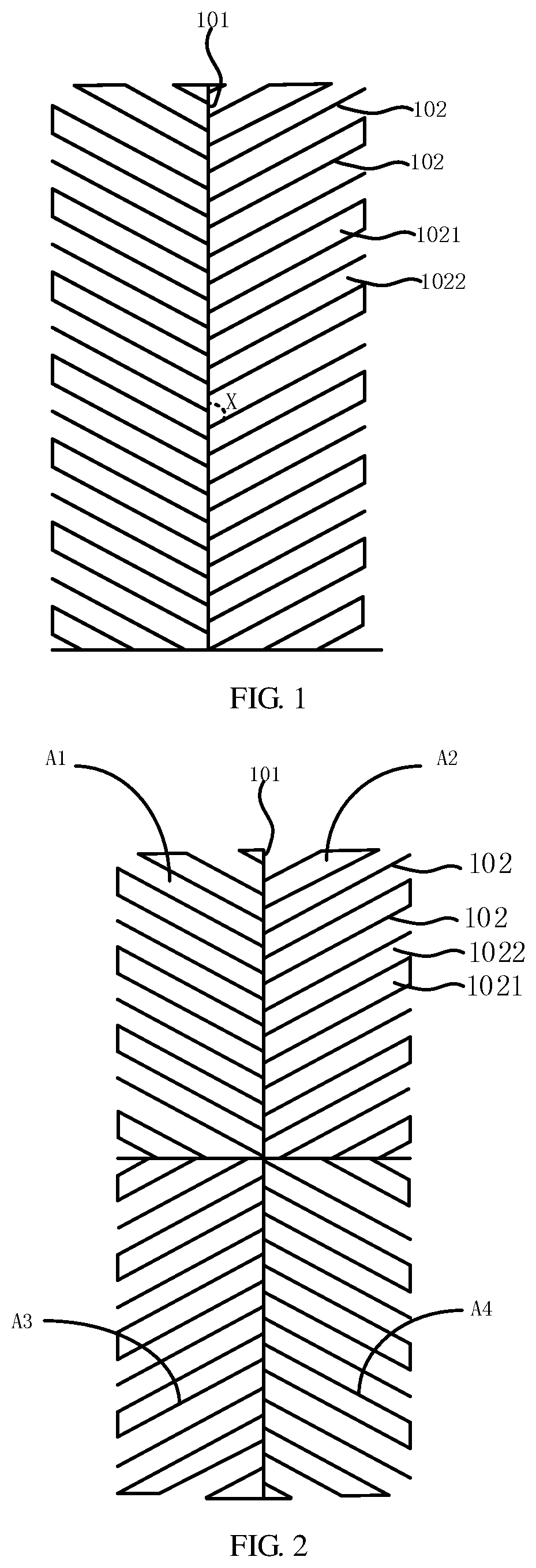
[0036]Referring to FIG. 1, FIG. 1 is a schematic diagram of a pixel structure according to an embodiment of the present invention, including:
[0037]a main electrode 101; and
[0038]a plurality of branch electrodes 102 connected to the main electrode 101;
[0039]wherein, closed areas 1021 and open areas 1022 are formed among the plurality of the branch electrodes 102, any of the closed areas is located between adjacent two of the plurality of branch electrodes, and any of the open areas is located between adjacent two of the plurality of branch electrodes.
[0040]In a specific embodiment, an intersecting angle X between any one of the branch electrodes 102 and the main electrode 101 is not equal to 90 degrees.
[0041]The main electrode 101 in the embodiment is strip-shaped, the two sides of the main electrode 101 are the branch electrodes 102, each branch electrode 102 is also strip-shaped, and is connected to the main electrode 101. A slit is formed between the gaps between each two adjacent...
embodiment 2
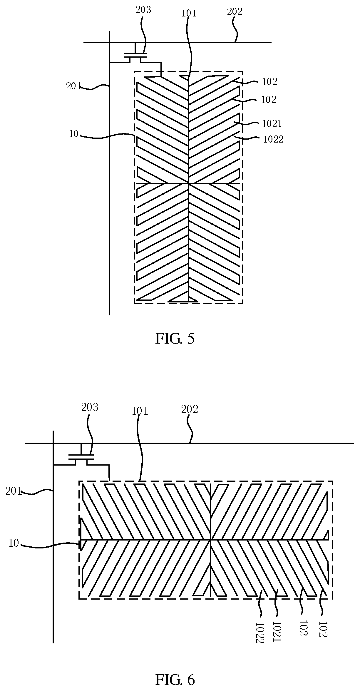
[0054]Referring to FIG. 5, FIG. 5 is a schematic diagram of a pixel unit according to an embodiment of the present invention.
[0055]The embodiment of the invention further provides a pixel unit, including:
[0057]a switch element 203, electrically connected with the data line 201 and the scan line 202; and
[0058]a pixel structure 10, electrically connected with the switch element 203;
[0059]wherein the pixel structure 10 includes: a main electrode 101, a plurality of branch electrodes 102 connected to the main electrode 101, and closed areas 1021 or open areas 1022 formed between the adjacent two branch electrodes 102.
[0060]In this embodiment, the data line 201 is disposed perpendicular to the scan line 202. It should be noted that, in this embodiment, the data line 201 and the scan line 202 carry a pixel structure 10 as an example. In an actual display panel, one scan line 202 and one data line 201 correspond to a plurality of pixel structures on w...
PUM
Abstract
The invention discloses a pixel structure including: a main electrode, and a plurality of branch electrodes connected to the main electrode; wherein closed areas and open areas are formed among the plurality of the branch electrodes. The invention solves the problem that the liquid crystal at the edge position of the peripheral closed design scheme is easily affected by the electric field and the alignment disorder occurs by designing the branchelectrode in the ITO electrode as the closed area and the open area, so that the display is uniform and the display effect is improved. Further, with respect to the design of the peripheral opening, the invention reduces the number of black streaks and increases the light transmittance due to the closed areas and the open areas of the interval distribution.
Description
FIELD OF THE DISCLOSURE[0001]The present invention relates to the field of display, and in particular to a pixel structure, a pixel unit, and a display panel.BACKGROUND OF THE DISCLOSURE[0002]As the display specifications of liquid crystal displays continue to develop toward large sizes, the market demands more and more attention to high contrast, rapid response, and wide viewing angles for the performance requirements of liquid crystal displays. In order to overcome the viewing angle problem of a large-sized liquid crystal display panel, the wide viewing angle technology of the liquid crystal display panel must be continuously improved. Polymer stabilized vertical alignment liquid crystal (PSVA) is one of the wide viewing angle technologies currently widely used in liquid crystal display panels.[0003]The ITO (IndiumTinOxide) electrode of the existing PSVA liquid crystal panel adopts a peripheral closed design method, and in this way, the liquid crystal at the edge of the ITO elec...
Claims
Application Information
Patent Timeline
Application Date:The date an application was filed.
Publication Date:The date a patent or application was officially published.
First Publication Date:The earliest publication date of a patent with the same application number.
Issue Date:Publication date of the patent grant document.
PCT Entry Date:The Entry date of PCT National Phase.
Estimated Expiry Date:The statutory expiry date of a patent right according to the Patent Law, and it is the longest term of protection that the patent right can achieve without the termination of the patent right due to other reasons(Term extension factor has been taken into account ).
Invalid Date:Actual expiry date is based on effective date or publication date of legal transaction data of invalid patent.

