Drive circuit and image forming apparatus using the same

a technology of drive circuit and image forming apparatus, which is applied in the direction of electric digital data processing, instruments, computing, etc., can solve the problem of difficulty in compensating for a change in luminance by a unit of frame for each pixel

Inactive Publication Date: 2009-03-10
CANON KK
View PDF16 Cites 236 Cited by
  • Summary
  • Abstract
  • Description
  • Claims
  • Application Information

AI Technical Summary

Benefits of technology

[0011]It is an object of the invention to provide a drive circuit that can drive a load stably for a long period of time, even if the load deteriorates with time to cause changes in an impedance and a resistance, and an image forming apparatus using the drive circuit.
[0012]It is another object of the invention, even in the case in which a load is a light-emitting element having a characteristic of deteriorating with time, to realize stable image formation for a long period of time by detecting a fall in luminance due to aged deterioration of the light-emitting element for each pixel, and correcting (compensating for) the fall in luminance.
[0018]Preferably, it is possible to multiply the correction signal with a coefficient according to a setting for a size of the transistor for correction.
[0028]According to the invention, even if a load deteriorates with time to cause changes in an impedance and a resistance, feedback provides stable drive over a long period of time.

Problems solved by technology

However, according to these proposals, the methods require means for storing a drive time and a sensor, and it is difficult to compensate for a change in a luminance by a unit of a frame for each pixel.

Method used


Image

  • Drive circuit and image forming apparatus using the same
  • Drive circuit and image forming apparatus using the same
  • Drive circuit and image forming apparatus using the same

Examples


first embodiment

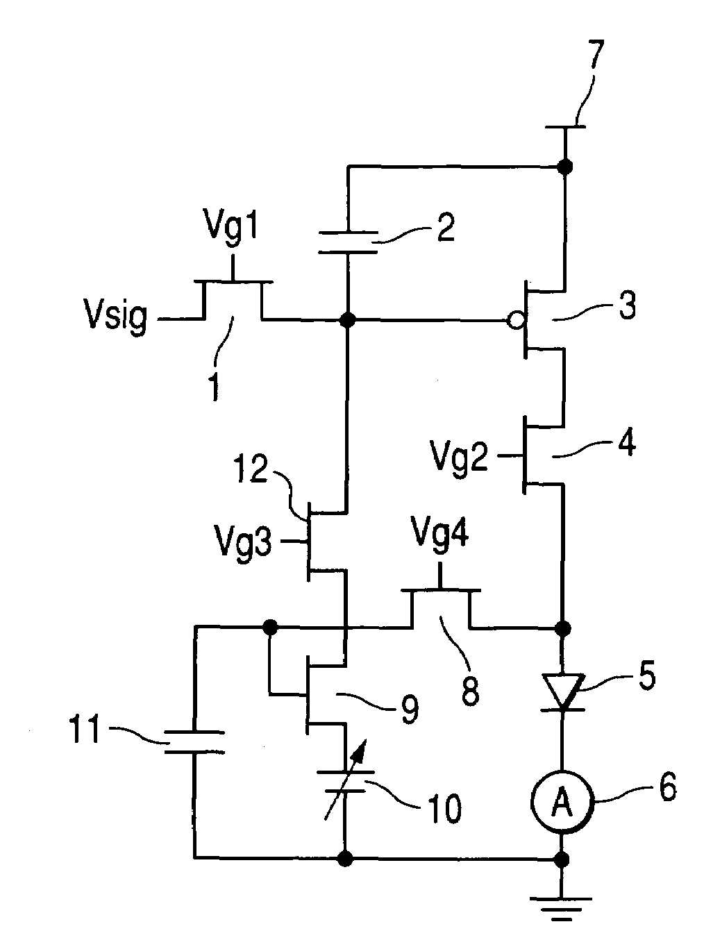
[0048]FIG. 1 shows a pixel circuit of an embodiment of a display element of the invention. As a load, a light-emitting element 5 is used. In the figure, reference numerals 1, 3, 4, 8, 9 and 12 denote TFTs. Only the TFT 3 is a p type and the other TFTs are an n type. Reference numerals 2 and 11 denote capacitors; reference numeral 6, an ammeter; reference numeral 7, a power supply; and reference numeral 10, a variable or fixed bias voltage supply. In the figure, the TFT 3 is a drive transistor and the TFT 9 is a second transistor. The ammeter 6 is unnecessary in an actual drive circuit.

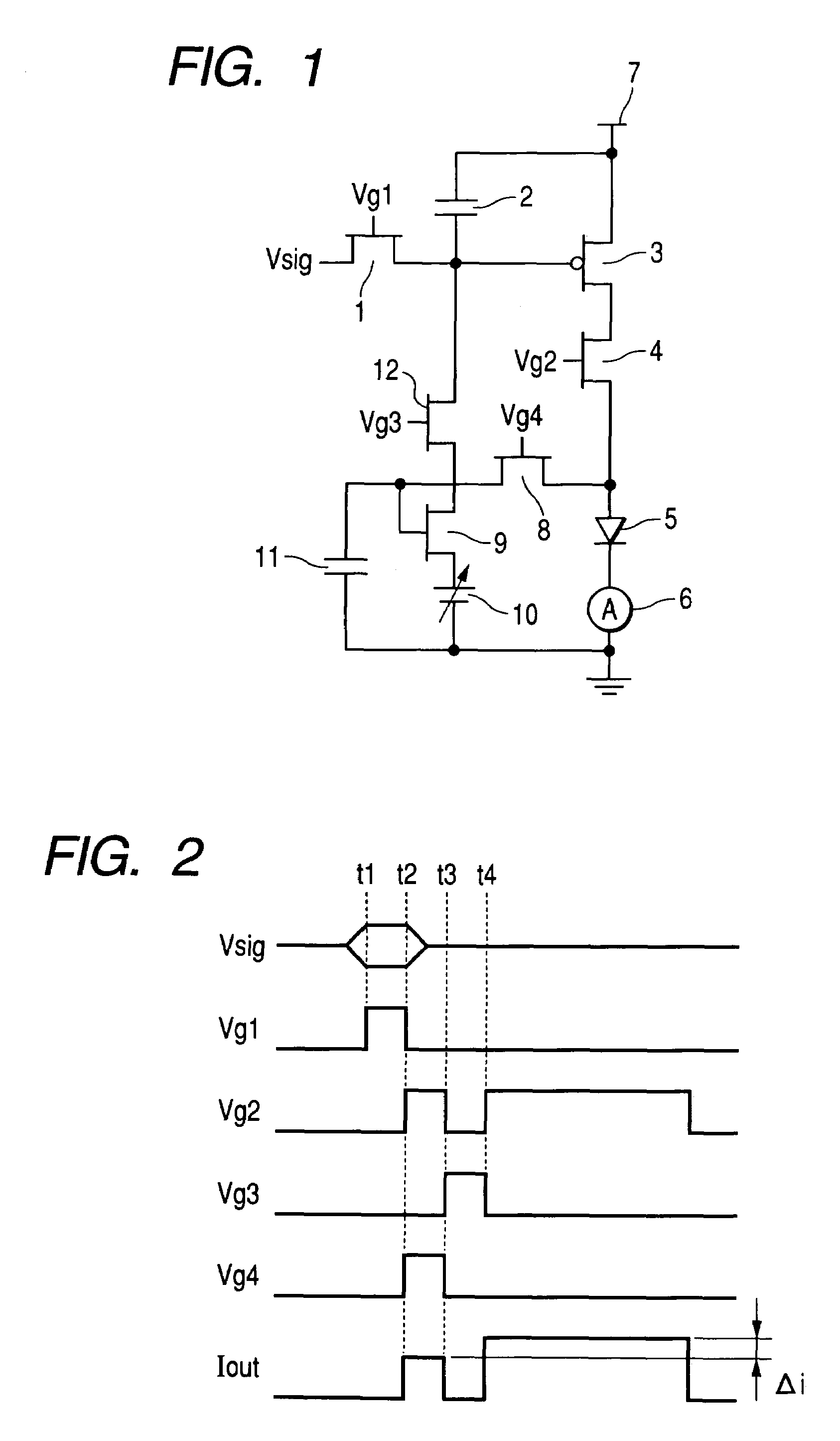
[0049]A drive circuit for the load of this embodiment is a voltage programming type. An input signal according to a voltage corresponding to a display luminance is applied to each pixel circuit as a display signal Vsig. An operation of the pixel will be explained according to a timing chart of FIG. 2.

[0050]The display signal Vsig corresponding to a luminance of a display in the next frame is inputted t...

second embodiment

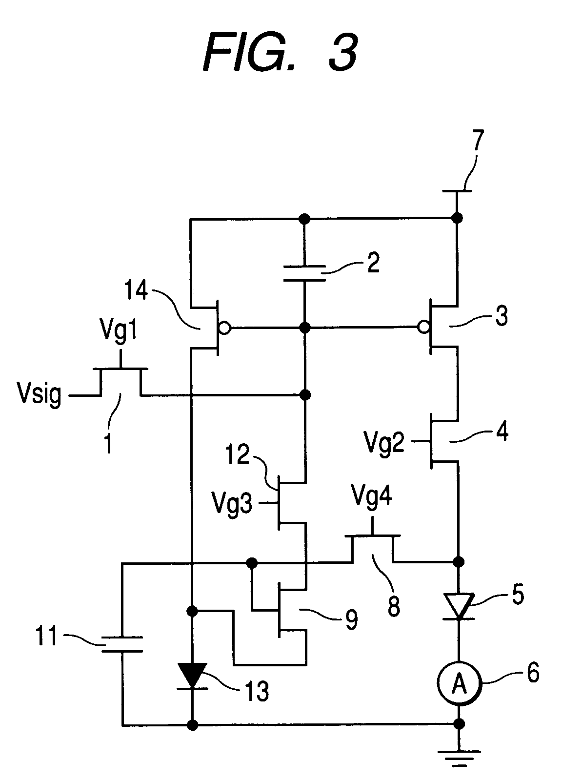
[0055]FIG. 3 shows a pixel circuit of a second embodiment of the display element of the invention. In the figure, reference numeral 12 denotes a nonlinear element having a diode characteristic and 14 denotes a p-type TFT. As a load, the light-emitting element 5 is used.

[0056]In the pixel circuit of this embodiment, the variable bias voltage 10 of the pixel circuit of the first embodiment is changed to a nonlinear element 13 and a current mirror circuit is constituted by the TFT 3 and TFT 14 serving as the drive transistors. An operation of this pixel circuit will be explained according to a timing chart of FIG. 2.

[0057]When a display signal is decided at time t1, Vg1 rises to H and the TFT 1 is turned ON, a charge corresponding to a display signal is accumulated in the capacitor 2, and gate potentials of the TFTs 3 and 14 are set. Subsequently, at the time t2, Vg1 falls to L and, at the same time, Vg2 and Vg4 rise to H, and the TFT 1 is turned OFF and the TFTs 4 and 8 are simultaneo...

third embodiment

[0060]FIG. 4 shows a pixel circuit of a third embodiment of the display element of the invention. In the figure, reference numerals 3, 14, 15 and 16 denote p-type TFTs and reference numerals 1, 8, 9, 12 and 17 denote n-type TFTs. As a load, the light-emitting element 5 is used.

[0061]The display element is a current programming type, and a display signal Idata, according to a current corresponding to a display luminance, is applied to each pixel circuit as an input signal. An operation of the pixel will be explained with reference to a timing chart shown in FIG. 5.

[0062]A display signal corresponding to a luminance of display in the next frame is inputted to an input terminal of the n-channel TFT 1, serving as a transistor for address, and, at decided time t1, gate potentials Vg1 and Vg6 of the TFTs 1 and 17 rise to H. At the same time, a gate potential Vg5 of the TFT 16 falls to L, the TFTs 1, 17 and 16 are turned ON and a charge corresponding to a voltage value of the display signa...


PUM


Abstract

A drive circuit including a drive transistor for feeding to a load a drive current corresponding to an input signal. The drive circuit has a correction circuit that supplies a correction signal corresponding to an impedance of the load to a gate of the drive transistor to correct the drive current to be fed to the load by the drive transistor, and in which the load is a light-emitting element. One terminal of the light-emitting element is connected to a gate of a transistor for correction, and when a predetermined potential Ps is set to a value calculated by deducting a threshold voltage Vth of the transistor for correction from a terminal potential Pi of the light-emitting element with respect to a drive current, the drive circuit sets a source potential of the transistor for correction to the predetermined potential Ps to thereby generate a voltage corresponding to an impedance of the light-emitting element as a source-to-drain current of the transistor for correction.

Description

[0001]This application claims priority from Japanese Patent Application No. 2004-035295, filed on Feb. 12, 2004, which is hereby incorporated by reference herein.BACKGROUND OF THE INVENTION[0002]1. Field of the Invention[0003]The present invention relates to a drive circuit for a load, which can be used in image forming apparatuses, represented by a television receiver, a digital camera, a digital video camera recorder, a monitor of a computer, a printer of an electrophotographic system, and the like. More specifically, the invention relates to a drive circuit for a light-emitting element that can be used in a display and an exposing device that uses a light-emitting element as a load.[0004]2. Related Background Art[0005]As an example of a load, a light-emitting element, in particular, an organic EL (electroluminescent) element is a planar self-luminous element of stacked thin film layers, which is capable of emitting light at a high luminance. This EL element makes it possible to e...

Claims


Application Information

Patent Timeline
Patent Type & Authority Patents(United States)
IPC IPC(8): G09G3/30G09G3/32
CPCG09G3/3233G09G3/3241G09G2300/0819G09G2300/0852G09G2300/0861G09G2300/088G09G2310/0254G09G2320/043G09G2320/045
Inventor YUKI, OSAMUNAKAJIMA, YOSHINORIKONDO, SHIGEKI
Owner CANON KK
Why Eureka
Try Eureka