Method and apparatus for image based power control of drive circuitry of a display pixel

a technology of drive circuitry and display pixel, which is applied in the field of flat panel displays, can solve the problems of component degradation, oled display elements degrade over time, and output progressively less ligh

Inactive Publication Date: 2007-01-11
LEADIS TECH
View PDF2 Cites 243 Cited by
  • Summary
  • Abstract
  • Description
  • Claims
  • Application Information

AI Technical Summary

Benefits of technology

[0008] The present invention relates to methods and apparatus for displaying an image having one or more frames. The display can be an organic light emitting diode (OLED) display. The display includes an active matrix of pixels including OLED circuitry. The display also includes a voltage source for providing a voltage to the OLED driver and a detection circuit for determining the maximum brightness level associated with an image frame. A control circuit for adjusting the voltage provided to the OLED driver according to the maximum brightness level determined by the detection circuit is also provided.

Problems solved by technology

However, a major problem with the OLED displays is that the OLED display elements degrade over time and output progressively less light.
That heat is undesirable because it results in the degradation of the components located near T2.

Method used


Image

  • Method and apparatus for image based power control of drive circuitry of a display pixel
  • Method and apparatus for image based power control of drive circuitry of a display pixel
  • Method and apparatus for image based power control of drive circuitry of a display pixel

Examples


Embodiment Construction

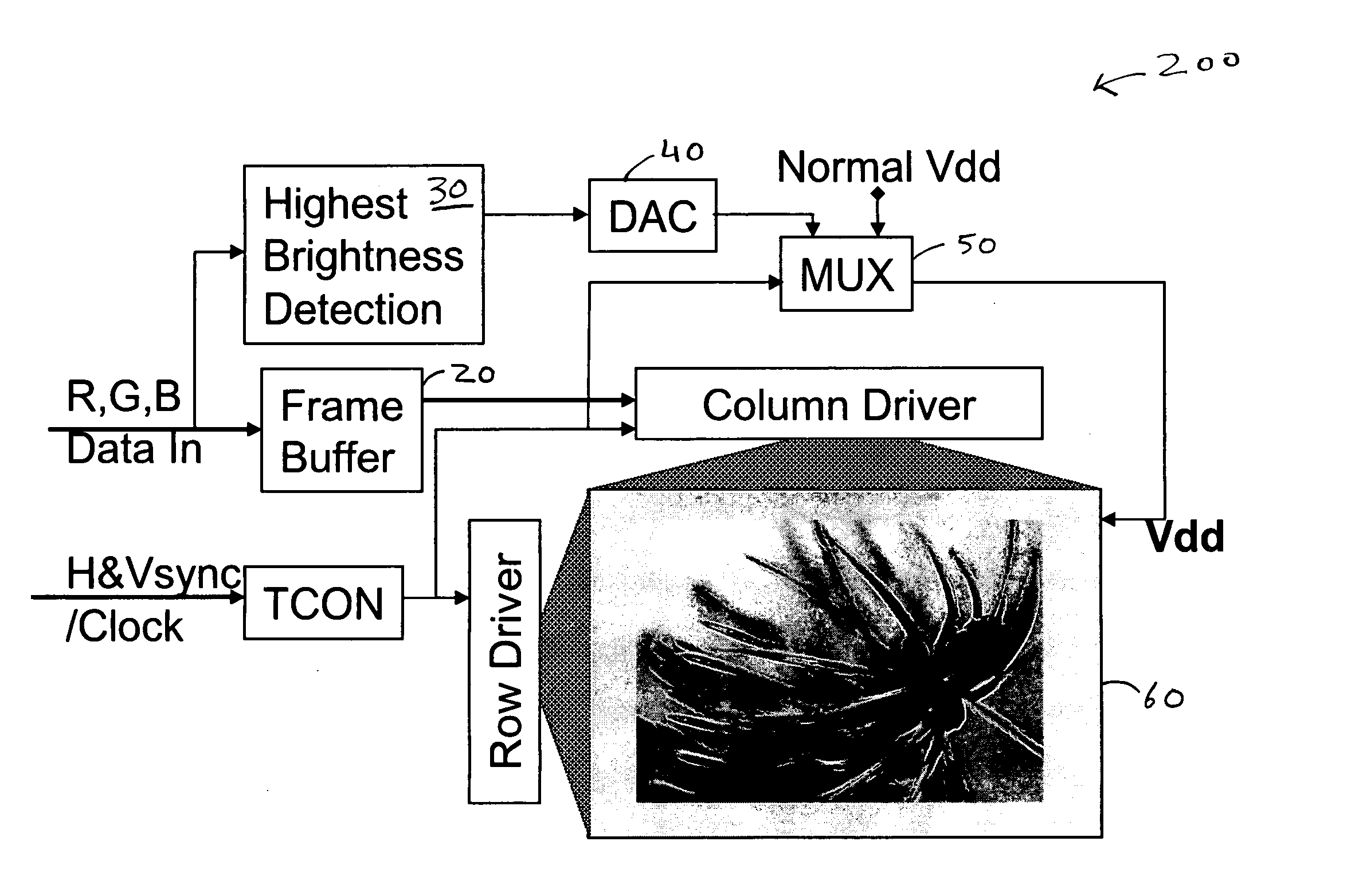
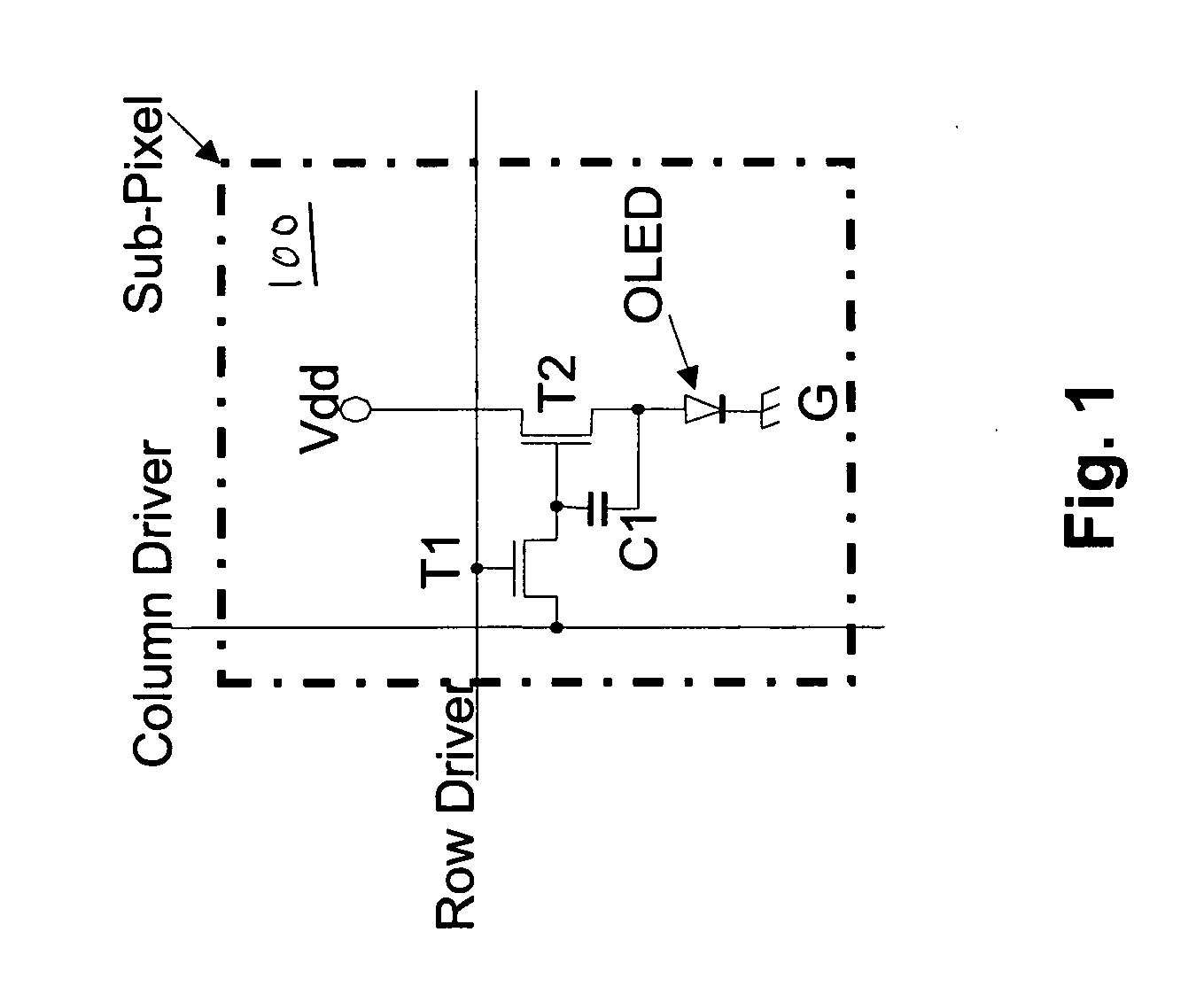
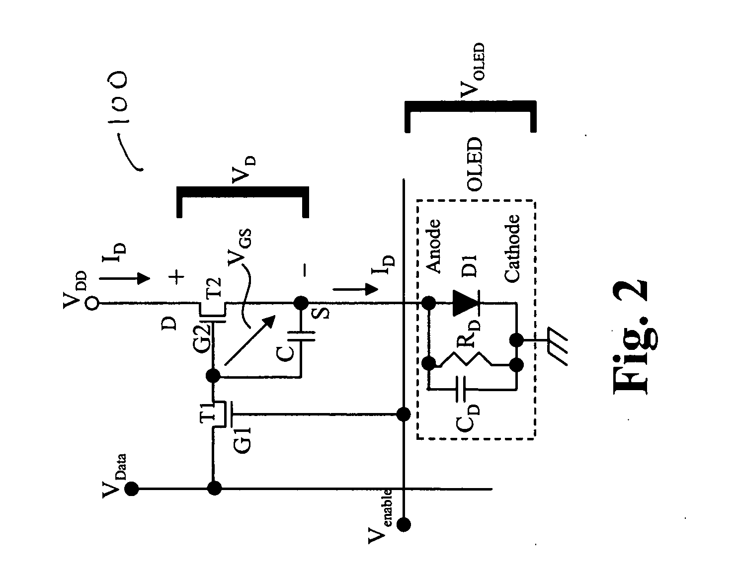
[0023] The present invention provides apparatus and methods to control and the reduce power provided to the OLED through T2 and thus reduces the heat dissipated by T2, thereby improving OLED life and preventing the degradation of the OLED circuitry elements. The power consumption of the OLED is minimized by reducing the OLED drive transistor drain voltage during display intervals that require less than full-scale worst case illumination. By reducing VDD when displaying dim brightness levels, the power and heat generated across T2 are reduced and that increases the OLED lifetime.

[0024] The VDD supply is common to all sub-pixels and pixels of the display. Because one sub-pixel could be displaying a dim brightness level while another sub-pixel displays a high brightness level, lowering the VDD for dim sub-pixels is not feasible in a system in which VDD is common to all sub-pixels. Therefore, the present invention uses a multiplexor associated with each pixel or sub-pixel to adjust the...


PUM


Abstract

An apparatus and a method for controllably reducing power and heat dissipated by OLED display circuitry are disclosed. Image dependent drive voltage adjustments are made to reduce the power generated by and the heat dissipated by the OLED pixel circuitry. That extends the life span of the components of the OLED pixel circuitry and maintains their quality by reducing or eliminating the degradation caused by heat. The apparatus and the method of the present invention selectively reduce the voltage level provided to the drain of the transistor used to drive the OLED. The drive transistor's drain voltage level is controllably lowered during display intervals that require less than the brightest level of illumination.

Description

RELATED APPLICATION [0001] The present application claims priority to the U.S. Provisional Patent Application No. 60 / 674,672, filed on Apr. 20, 2005.FIELD OF INVENTION [0002] This invention relates to flat panel displays and more specifically to Organic Light Emitting Diode (OLED) type displays. BACKGROUND OF THE INVENTION [0003] Flat panel displays including plasma, electroluminescent (EL), organic light emitting diode (OLED) and liquid crystal displays are used in a variety of products ranging from cell phones and personal digital assistants (PDA) to computers and televisions. Active Matrix Liquid Crystal Displays (AMLCD) are known in the art. In the active matrix displays, the row driver and the column driver are used to control the OLED pixel, and a capacitor is used to continue to drive the pixel when the drivers are not driving the pixel because they are driving other pixels. The AMLCD can produce about 16 million different colors by carefully controlling the voltages provided...

Claims


Application Information

Patent Timeline
Patent Type & Authority Applications(United States)
IPC IPC(8): G09G5/00
CPCG09G3/3233G09G2300/0842G09G2320/0673G09G2360/16G09G2360/18H05B33/0896G09G2330/021H05B45/60Y02B20/30
Inventor BASSETTI, CHESTER FLOYD
Owner LEADIS TECH
Why Eureka
Try Eureka