Power module package
a power module and package technology, applied in semiconductor devices, multilayer circuit manufacturing, semiconductor/solid-state device details, etc., can solve the problems of reducing the use of manufacturing coats, and reducing the use of wires.
- Summary
- Abstract
- Description
- Claims
- Application Information
AI Technical Summary
Benefits of technology
Problems solved by technology
Method used
Image

Examples
first preferred embodiment
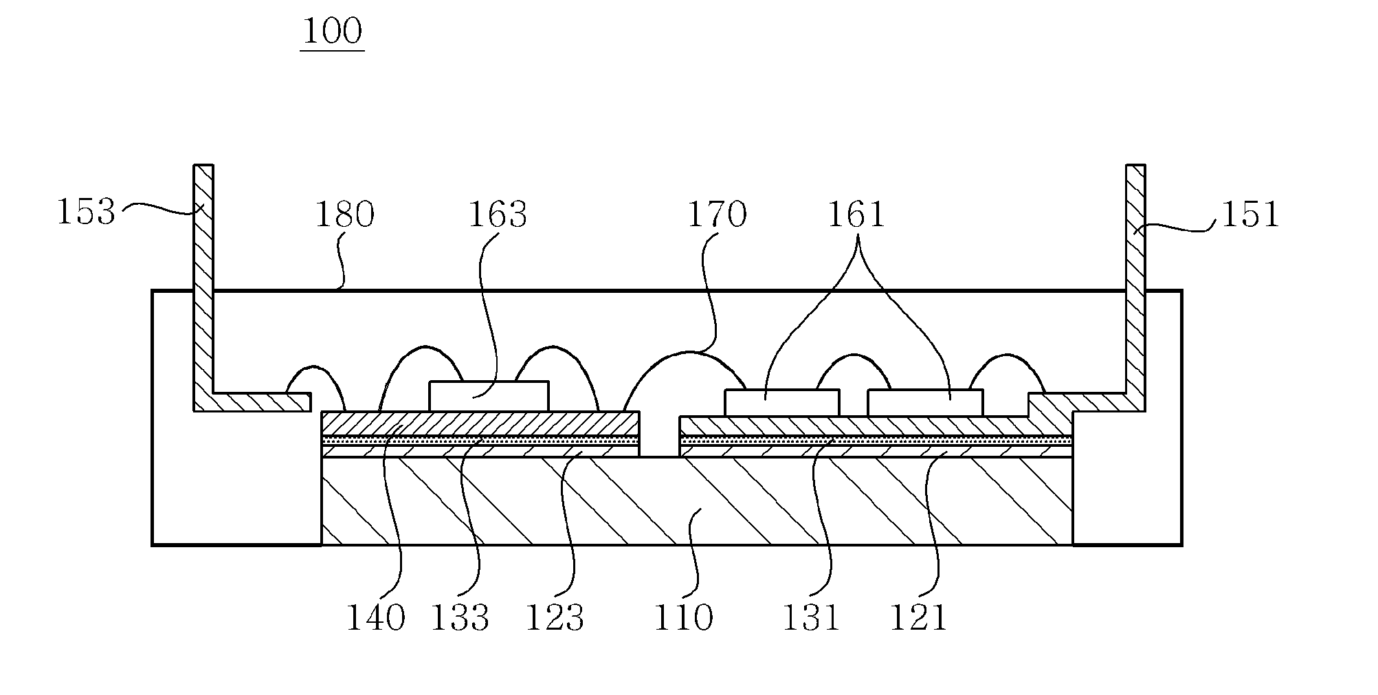
[0046]FIG. 1 is a cross-sectional view showing a structure of a power module package according to a first preferred embodiment of the present invention.
[0047]Referring to FIG. 1, the power module package 100 according to the first preferred embodiment of the present invention includes a first substrate 110, a second substrate 140, and a first lead frame 151.
[0048]The first substrate 110 may have one surface and the other surface. One surface means an ‘upper substrate’, and the other surface means a ‘lower surface’, based on FIG. 1. Hereinafter, each of one surface and the other surface will be referred to as the ‘upper surface’ and the ‘lower surface.
[0049]According to the present embodiment, the first substrate 110 may be a ceramic substrate, but is not particularly limited thereto. That is, the first substrate 110 may include a metal substrate having an anodized layer, a printed circuit board, and a direct bonded copper (DBC) substrate, or the like.
[0050]The ceramic substrate may ...
second preferred embodiment
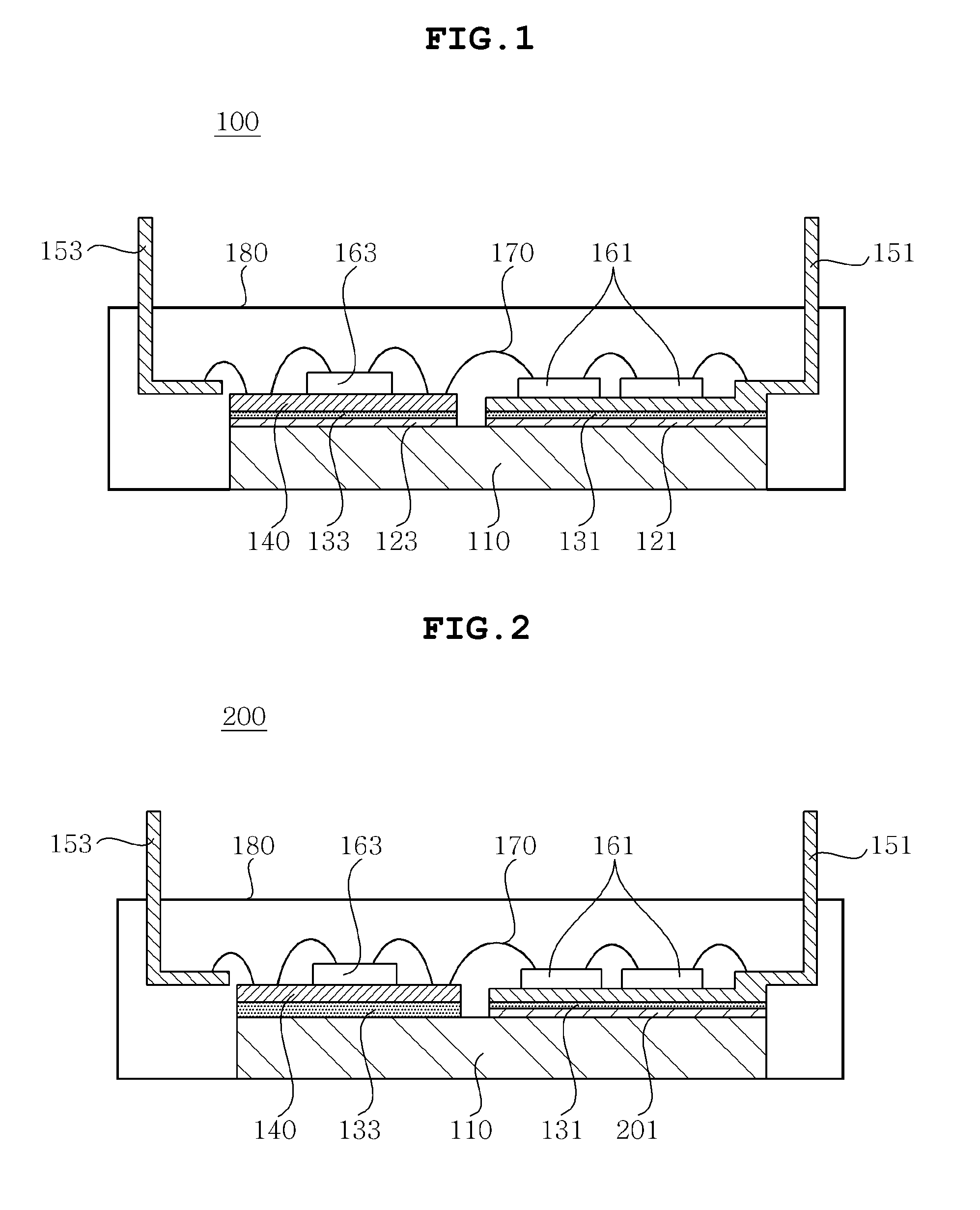
[0079]FIG. 2 is a cross-sectional view showing a structure of a power module package according to a second preferred embodiment of the present invention.
[0080]In the present embodiment, a description of components overlapped with the components described in the first preferred embodiment will be omitted. In addition, the same reference numerals will be used to describe the same components as the components described in the first preferred embodiment.
[0081]Referring to FIG. 2, in the power module package 200 according to the present embodiment, a first bonding layer 133 may be formed between one side of an upper surface of a first substrate 110 and a second substrate 140, and a metal layer 201 and a second bonding layer 131 may be formed between the other side of the upper surface of the first substrate 110 and a first lead frame 151, unlike the first preferred embodiment described above.
[0082]Here, the first bonding layer 133 may be made of a bonding material such as non-conductive ...
third preferred embodiment
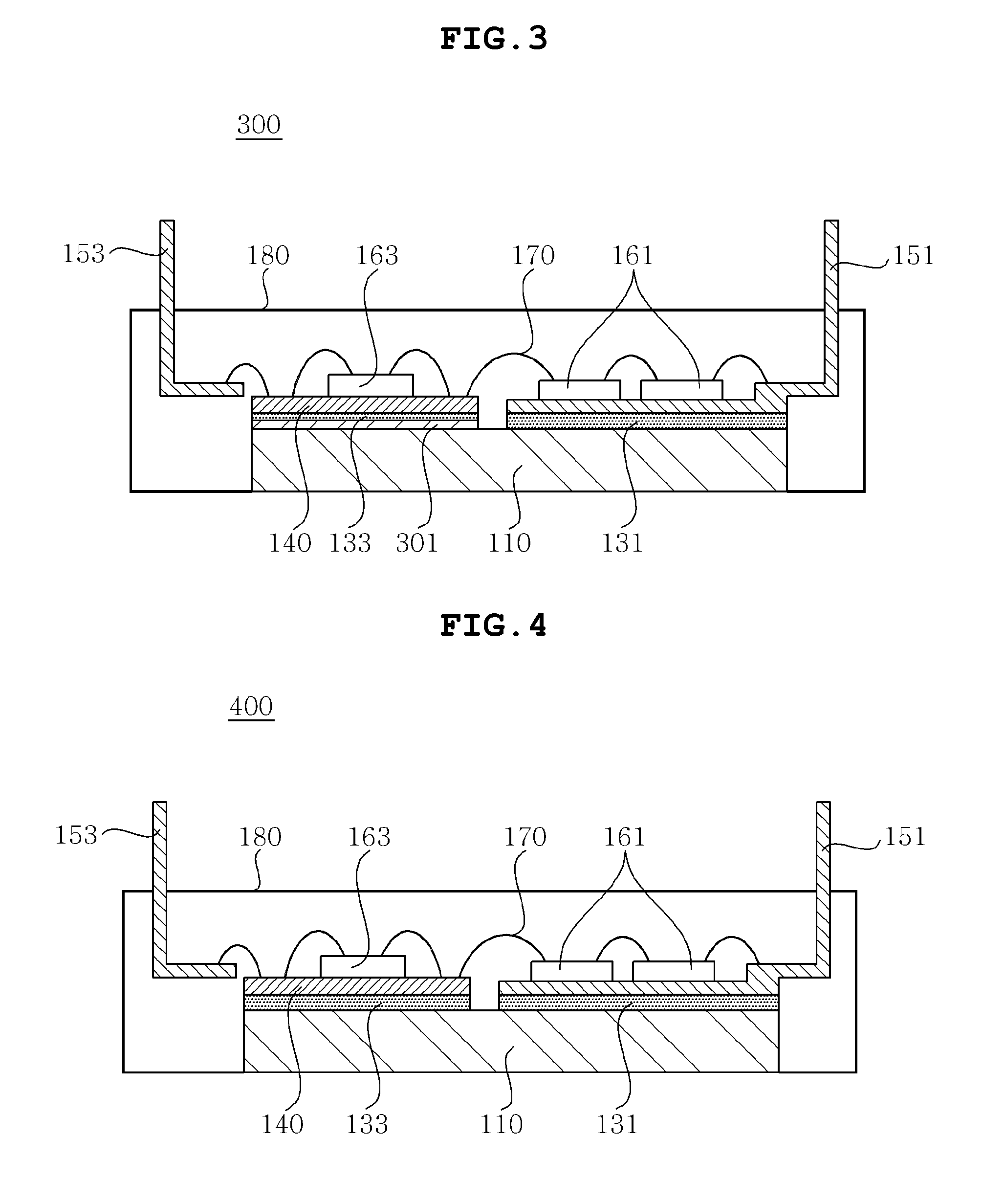
[0085]FIG. 3 is a cross-sectional view showing a structure of a power module package according to a third preferred embodiment of the present invention.
[0086]In the present embodiment, a description of components overlapped with the components described in the first preferred embodiment will be omitted. In addition, the same reference numerals will be used to describe the same components as the components described in the first preferred embodiment.
[0087]Referring to FIG. 3, in the power module package 300 according to the present embodiment, a metal layer 301 and a first bonding layer 133 may be formed between one side of an upper surface of a first substrate 110 and a second substrate 140, and a second bonding layer 131 may be formed between the other side of the upper surface of the first substrate 110 and a first lead frame 151, unlike the first preferred embodiment described above.
[0088]Here, the second bonding layer 131 may be made of conductive epoxy having high thermal condu...
PUM
 Abstract
Description
Claims
Application Information
 - R&D Engineer
- R&D Manager
- IP Professional
- Industry Leading Data Capabilities
- Powerful AI technology
- Patent DNA Extraction
Browse by: Latest US Patents, China's latest patents, Technical Efficacy Thesaurus, Application Domain, Technology Topic.
© 2024 PatSnap. All rights reserved.Legal|Privacy policy|Modern Slavery Act Transparency Statement|Sitemap