Method for monitoring devices in semiconductor process

Inactive Publication Date: 2013-05-30
SHANGHAI HUALI MICROELECTRONICS CORP
View PDF13 Cites 4 Cited by
  • Summary
  • Abstract
  • Description
  • Claims
  • Application Information

AI Technical Summary

Benefits of technology

The present invention provides a method for monitoring devices in semiconductor processes to improve product yield. The method ensures even distribution of sampling lots to each process device, which reduces potential risks in the process.

Problems solved by technology

The fabrication of the semiconductor integrated circuits involves hundreds of process steps and any of these steps out of monitoring may cause end-of-line IC fail even other steps are well controlled.
Therefore, monitoring each process step and performing early warnings is one of the critical issues for semiconductor integrated process.
However, both the monitoring methods have limitations and risk periods which cause uncertainties in production.
Off-line monitoring can only be implemented when the tool is not in operation, thus the frequency of monitoring is low and the uncertainties in production cannot be monitored in time.
In-line monitoring is part of the whole process but usually cannot inspect all the wafers.
Therefore, wafers processed by a certain process tool may never be inspected which causes the process tool out of monitoring for a time and enlarges the risk.
Consequently, conventional semiconductor factories utilizing the sampling inspection method mentioned above may take the risk generated by the large amount of wafers which skip the inspection in production.

Method used


Image

  • Method for monitoring devices in semiconductor process
  • Method for monitoring devices in semiconductor process

Examples


Embodiment Construction

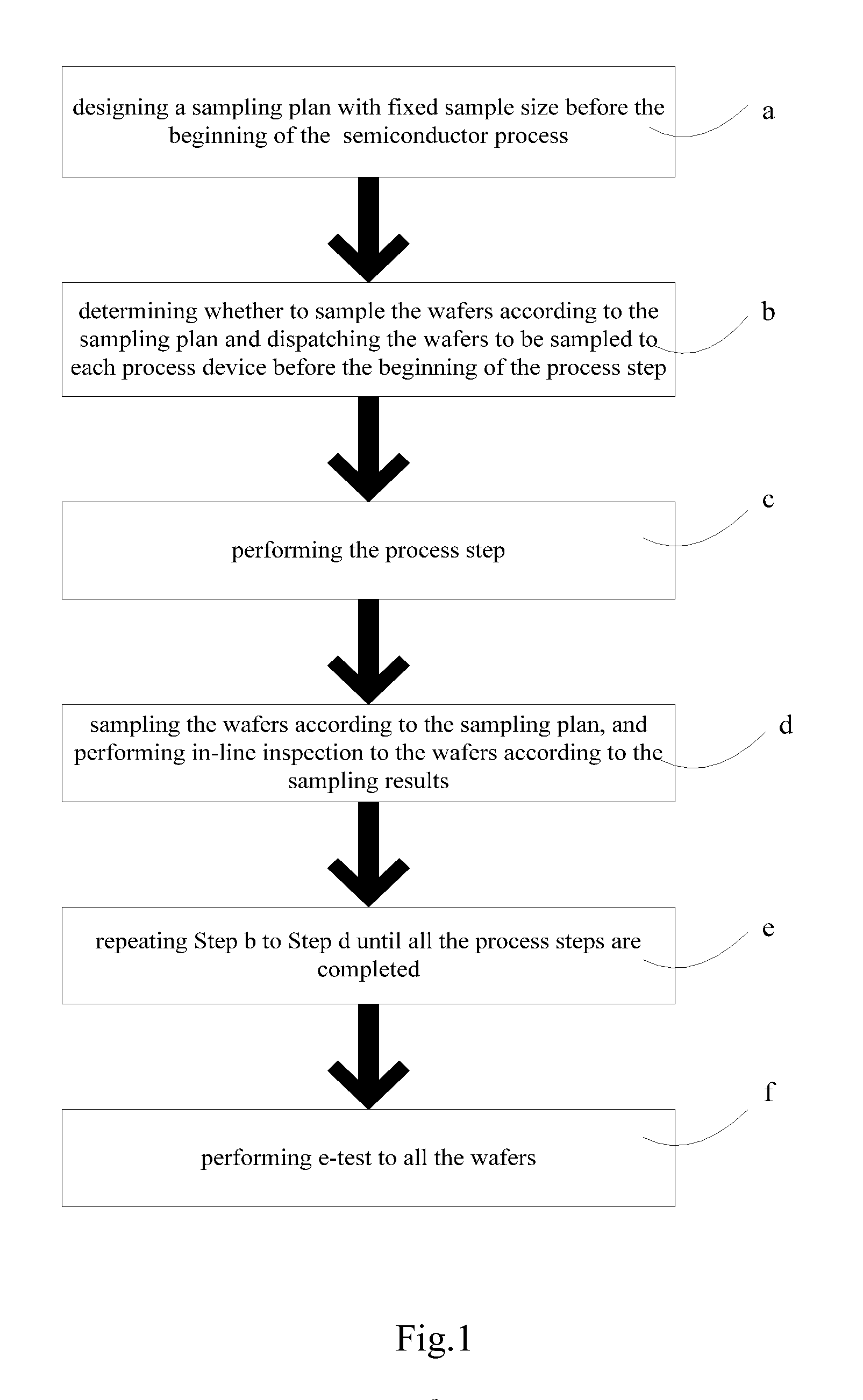
[0028]The method for monitoring devices in semiconductor process of the present invention will be described in further details hereinafter with respect to the embodiments and the accompanying drawings.

[0029]Referring to FIG. 1, the method for monitoring devices in semiconductor process comprises the following steps:

[0030]Step a, designing a sampling plan with fixed sample size before the beginning of the semiconductor process;

[0031]Step b, determining whether to sample the wafers according to the sampling plan and dispatching the wafers to be sampled to each process device evenly before the beginning of the process step, wherein the process device is used for performing the process step;

[0032]Step c, performing the process step;

[0033]Step d, sampling the wafers according to the sampling plan, and performing in-line inspection to the sampled wafers according to the sampling results;

[0034]Step e, repeating Step b to Step d until all the process steps are completed;

[0035]Step f, perfor...


PUM


Abstract

The invention provides a method for monitoring devices in semiconductor process comprising: Step a, designing a sampling plan with fixed sample size before the beginning of the semiconductor process; Step b, determining whether to sample the wafers according to the sampling plan and dispatching the wafers to be sampled to each process device before the beginning of the process step, wherein the process device is used for performing the process step; Step c, performing the process step; Step d, sampling the wafers according to the sampling plan, and performing in-line inspection to the sampled wafers according to the sampling results; Step e, repeating Step b to Step d until all the process steps are completed; Step f, performing e-test to all the wafers. According to the method, the potential risk during the semiconductor process can be minimized through the coordination of the sampling plan and the dynamic risk flag.

Description

CROSS-REFERENCE TO RELATED APPLICATION[0001]This application claims the priority benefit of China application serial no. 201110384000.2, filed Nov. 28, 2011. All disclosure of the China application is incorporated herein by reference.FIELD OF THE INVENTION[0002]The present invention relates to a monitoring method in semiconductor manufacturing process, and more particularly to a method for monitoring devices in semiconductor.BACKGROUND OF THE INVENTION[0003]The fabrication of the semiconductor integrated circuits involves hundreds of process steps and any of these steps out of monitoring may cause end-of-line IC fail even other steps are well controlled. Therefore, monitoring each process step and performing early warnings is one of the critical issues for semiconductor integrated process.[0004]The conventional semiconductor factories adopt off-line monitoring and in-line monitoring to inspect the process tool performance during the operation. However, both the monitoring methods ha...

Claims


Application Information

Patent Timeline
IPC IPC(8): H01L21/66
CPCH01L22/10H01L22/20H01L22/14
Inventor CHEN, HUNGLINWANG, KAIZHU, LUJUNNI, QILIANGLONG, YINGUO, MINGSHENG
Owner SHANGHAI HUALI MICROELECTRONICS CORP
Why Eureka
Try Eureka