Semiconductor FET and Method for Manufacturing the Same

Inactive Publication Date: 2013-08-29
INST OF MICROELECTRONICS CHINESE ACAD OF SCI
View PDF4 Cites 42 Cited by
  • Summary
  • Abstract
  • Description
  • Claims
  • Application Information

AI Technical Summary

Benefits of technology

[0026]By means of the semiconductor FET and the method for manufacturing the same of the present invention, a novel semiconductor FET structure is obtained, in which an airgap is form around the gate wall, and especially an airgap is formed between the gate wall and the contact wall. Due to the existence of this air

Problems solved by technology

The reason lies in that a FinFET is very small in size, and the process complexity would greatly increase if the separate cylindrical contact plug in the planar device is stilled adopted.
However, when the contact wall is used to replace the contact plug, a problem occurs in which a enormous para

Method used


Image

  • Semiconductor FET and Method for Manufacturing the Same
  • Semiconductor FET and Method for Manufacturing the Same
  • Semiconductor FET and Method for Manufacturing the Same

Examples


Embodiment Construction

[0034]Firstly, it should be noted that terms regarding position and orientation in the present invention, such as “above”, “below”, “left” and “right” etc, refer to the direction as viewed from the front of the sheet in which the drawings are located. Therefore, the terms “above”, “below”, “left” and “right”, etc regarding position and orientation in the present invention only indicate the relative positional relationship in cases as shown in the drawings. They are presented only for purpose of illustration, rather than limiting the scope of the present invention.

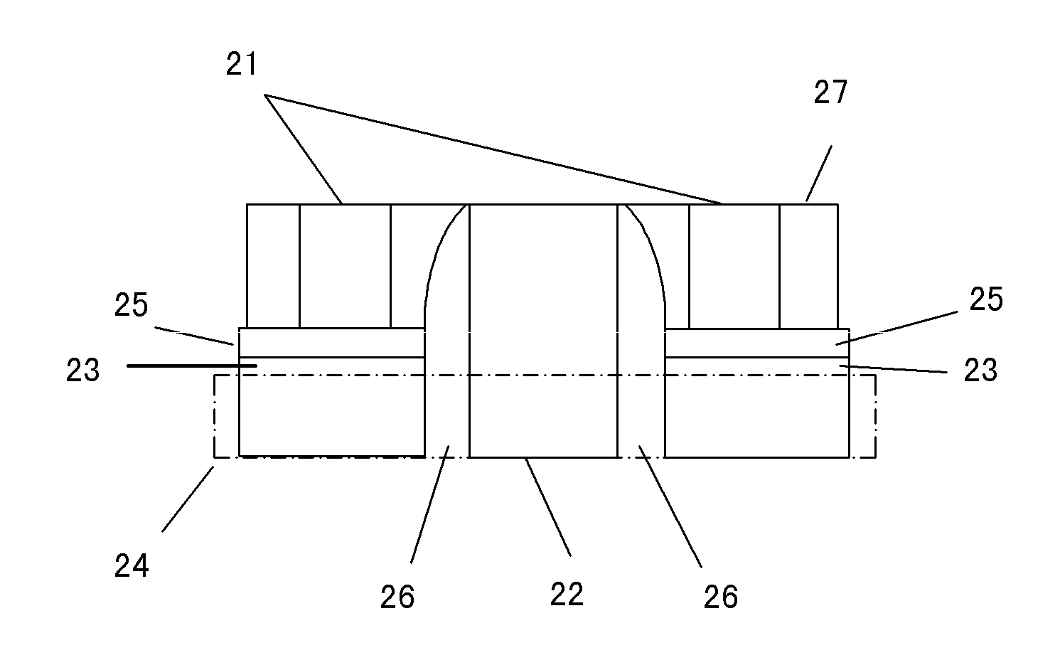
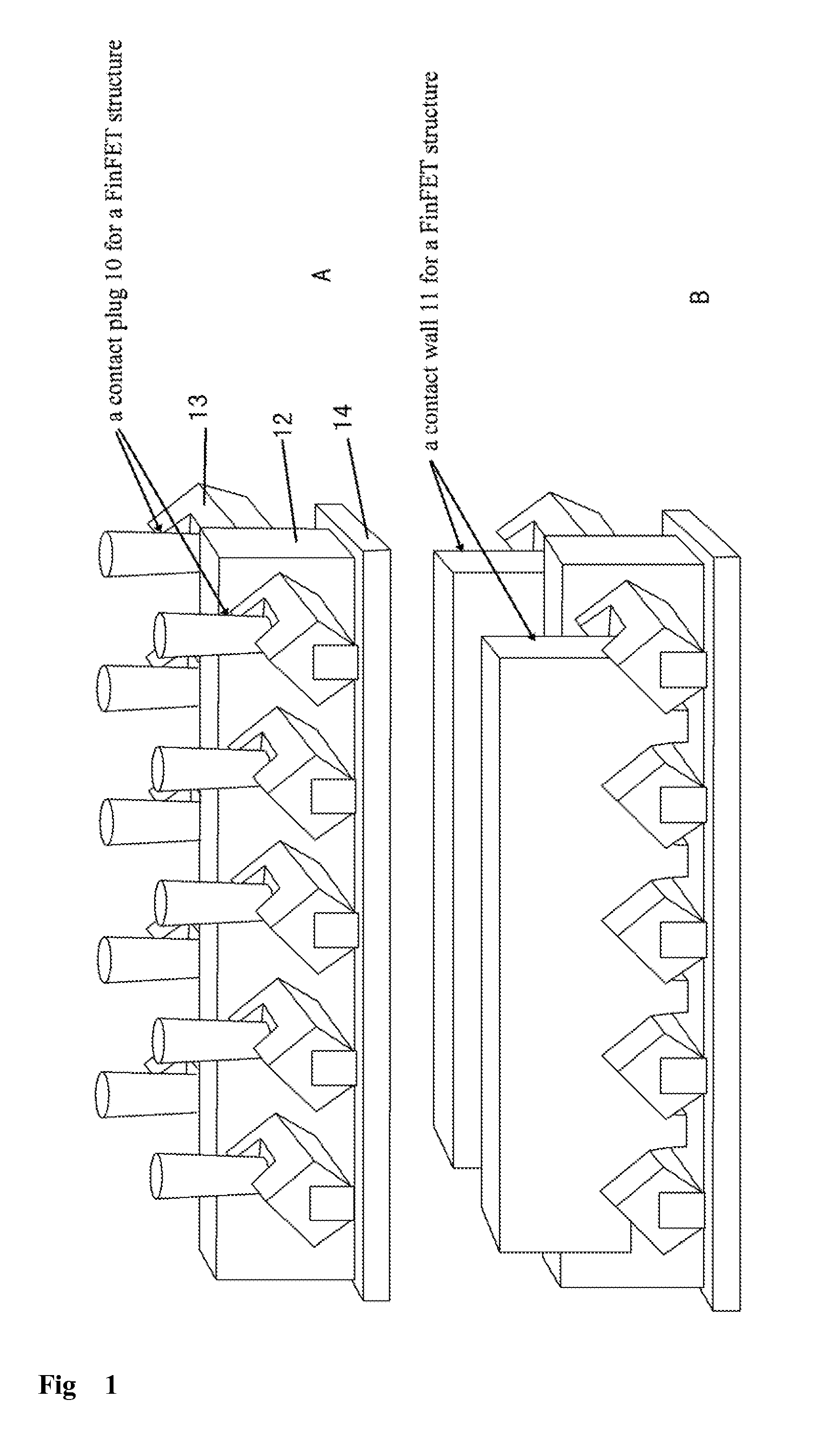
[0035]FIG. 1 schematically shows a contact plug and a contact wall used for a fin FET (FinFET) structure in the prior art. FIG. 1A shows a contact plug 10 for a FinFET structure known in the prior art. The contact plug 10 is located above the source / drain regions 13, and the gate wall 12 lies between a plurality of contact plugs 10. Both the contact wall 12 and the source / drain regions 13 are located on a common substrate 1...


PUM


Abstract

The present invention provides a semiconductor FET and a method for manufacturing the same. The semiconductor FET may comprise: a gate wall; a fin outside the gate wall, both ends of the fin being connected with the source/drain regions on both ends of the fin; and a contact wall on both sides of the gate wall, the contact wall being connected with the source/drain regions via the underlying silicide layer, wherein an airgap is provided around the gate wall. Since an airgap is formed around the gate wall, and particularly the airgap is formed between the gate wall and the contact wall, it is possible to decrease the parasitic capacitance between the gate wall and the contact wall. As a result, the problem of excessive parasitic capacitance resulting from use of the contact wall can be effectively alleviated.

Description

FIELD OF THE INVENTION[0001]The present invention generally relates to a semiconductor technology, and more particularly to a semiconductor Field Effect Transistor (FET) and a method for manufacturing the same.BACKGROUND OF THE INVENTION[0002]With progress in the semiconductor technology, Metal Oxide Semiconductor Field Effect Transistors (MOSFETs) with new structures have been developed continuously by the skilled person in the art. For example, Intel Corporation announced in 2011 that a tri-gate structure would be used in the 22 nm technical node. This three dimensional or 3-D transistor structure is also called as a fin FET (FinFET) or multiple gate (Multi-gate) FET.[0003]As for these three dimensional transistor structures, it is required to modify the contact accordingly. The reason lies in that a FinFET is very small in size, and the process complexity would greatly increase if the separate cylindrical contact plug in the planar device is stilled adopted. The contact plug may ...

Claims


Application Information

Patent Timeline
IPC IPC(8): H01L29/78H01L21/336
CPCH01L29/66795H01L2029/7858H01L29/785
Inventor ZHAO, CHAOLUO, JUNZHONG, HUICAI
Owner INST OF MICROELECTRONICS CHINESE ACAD OF SCI
Why Eureka
Try Eureka