Betavoltaic power sources for mobile device applications
- Summary
- Abstract
- Description
- Claims
- Application Information
AI Technical Summary
Benefits of technology
Problems solved by technology
Method used
Image

Examples
example energy conversion
Layer
[0105]FIGS. 6A and 6B are schematic diagrams (side view and top view, respectively) of an example embodiment of a diode-based energy conversion layer 10 for betavoltaic power source 6. The energy conversion layer 10 has a top 12 and a bottom 14. FIGS. 6A and 6B illustrate an example orientation of positive and negative electrodes 120P and 120N. Energy conversion layer 10 includes a P-doped layer 10P and an N-doped layer 10N separated by a P / N junction layer 10J.
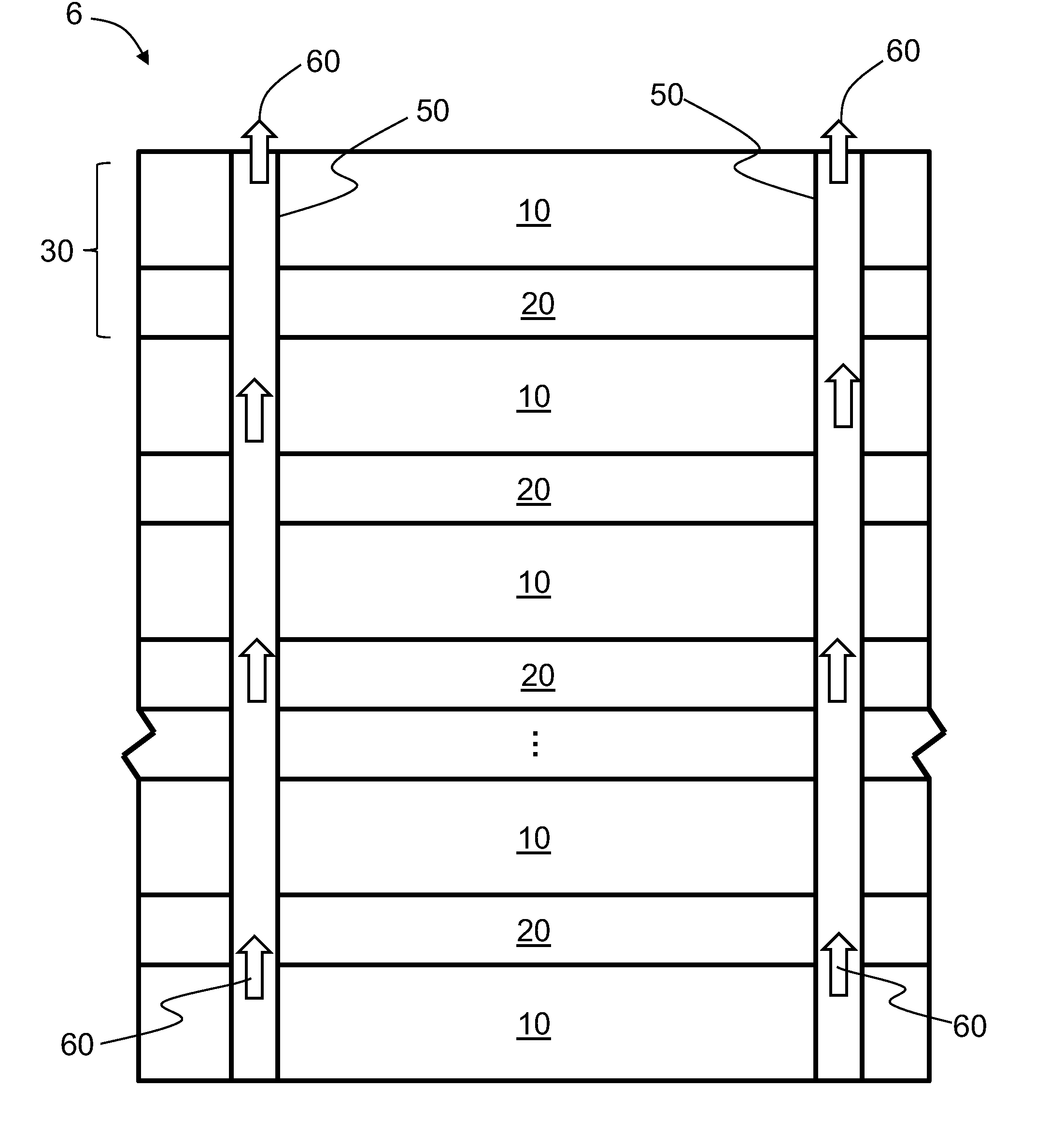
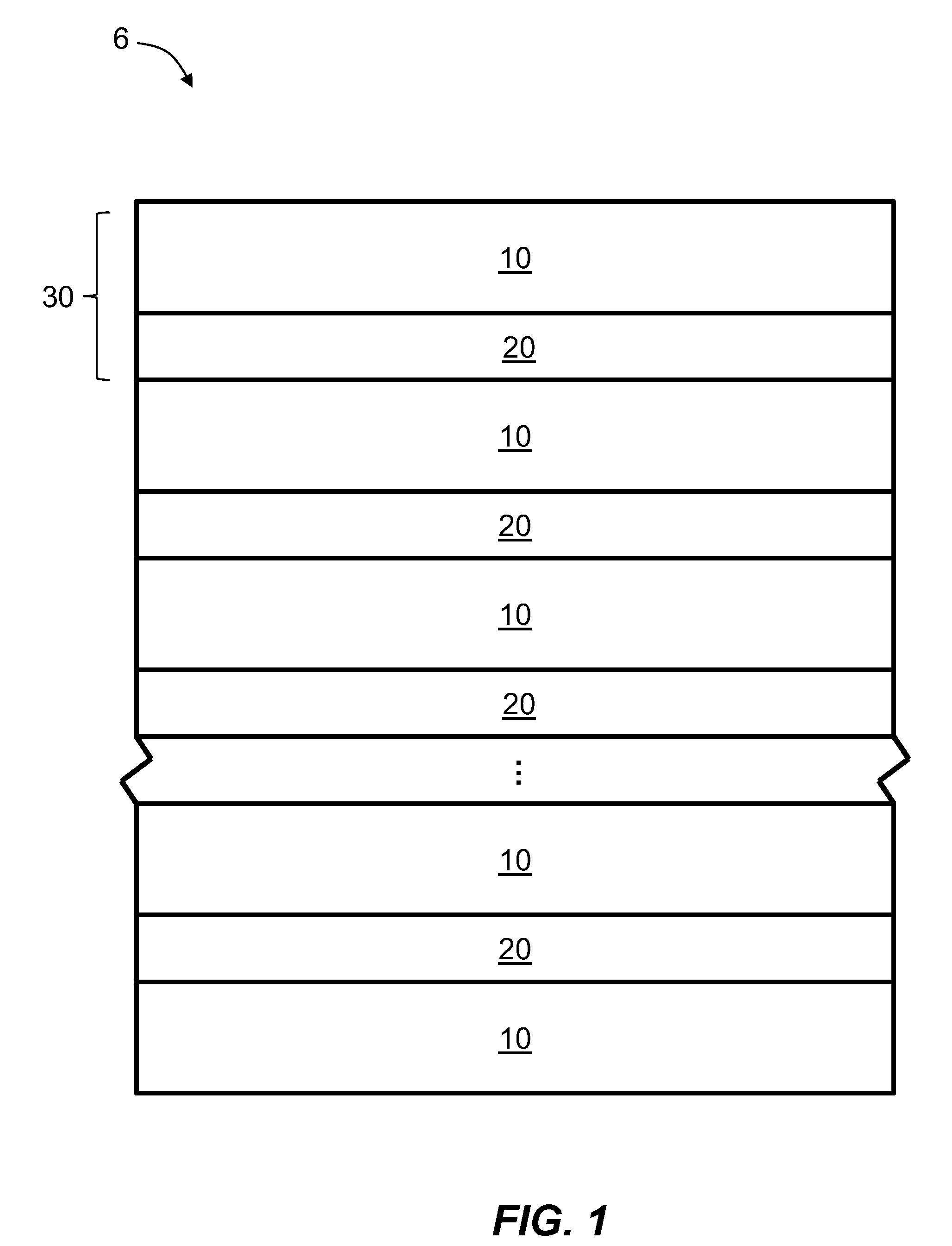
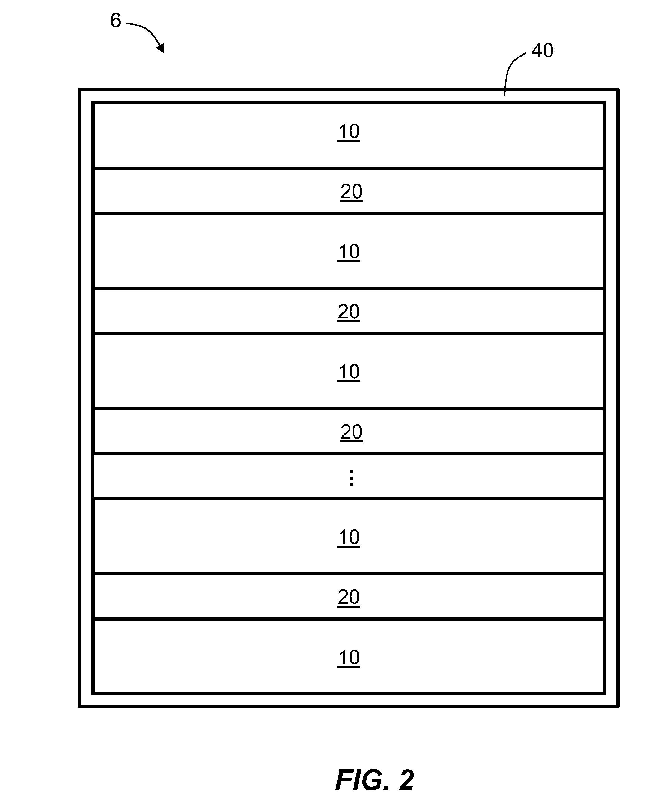
[0106]The positive and negative electrodes 120P and 120N can be positioned to allow for easy integration with isotope layers 20 (e.g., at the top and bottom of energy conversion layer 10 and on the same side, but offset, as shown). FIGS. 7A and 7B are respective side views that illustrate an example embodiment of a betavoltaic power source 6 having a multilayer stack configuration. FIG. 7C is a side view of the betavoltaic power source 6 as shown electrically connected via electrical leads (wires) 104 to external device ...
PUM
 Abstract
Description
Claims
Application Information
 - R&D
- Intellectual Property
- Life Sciences
- Materials
- Tech Scout
- Unparalleled Data Quality
- Higher Quality Content
- 60% Fewer Hallucinations
Browse by: Latest US Patents, China's latest patents, Technical Efficacy Thesaurus, Application Domain, Technology Topic, Popular Technical Reports.
© 2025 PatSnap. All rights reserved.Legal|Privacy policy|Modern Slavery Act Transparency Statement|Sitemap|About US| Contact US: help@patsnap.com