Conductive oxide film, display device, and method for forming conductive oxide film

Active Publication Date: 2014-03-06
SEMICON ENERGY LAB CO LTD
View PDF7 Cites 30 Cited by
  • Summary
  • Abstract
  • Description
  • Claims
  • Application Information

AI Technical Summary

Benefits of technology

[0054]A conductive oxide film having high conductivity and high transmittance of visible light can be obtained in the following manner: a conductive oxide film is formed at a high substrate temperature and the film is then subjected to nitrogen annealing treatment. In addition, a conductive oxide film having a crystal structure in which c-axes are aligned in a direct

Problems solved by technology

In other words, the tradeoff for either one of high conductivity and high transmittan

Method used


Image

  • Conductive oxide film, display device, and method for forming conductive oxide film
  • Conductive oxide film, display device, and method for forming conductive oxide film
  • Conductive oxide film, display device, and method for forming conductive oxide film

Examples


Example

Embodiment 1

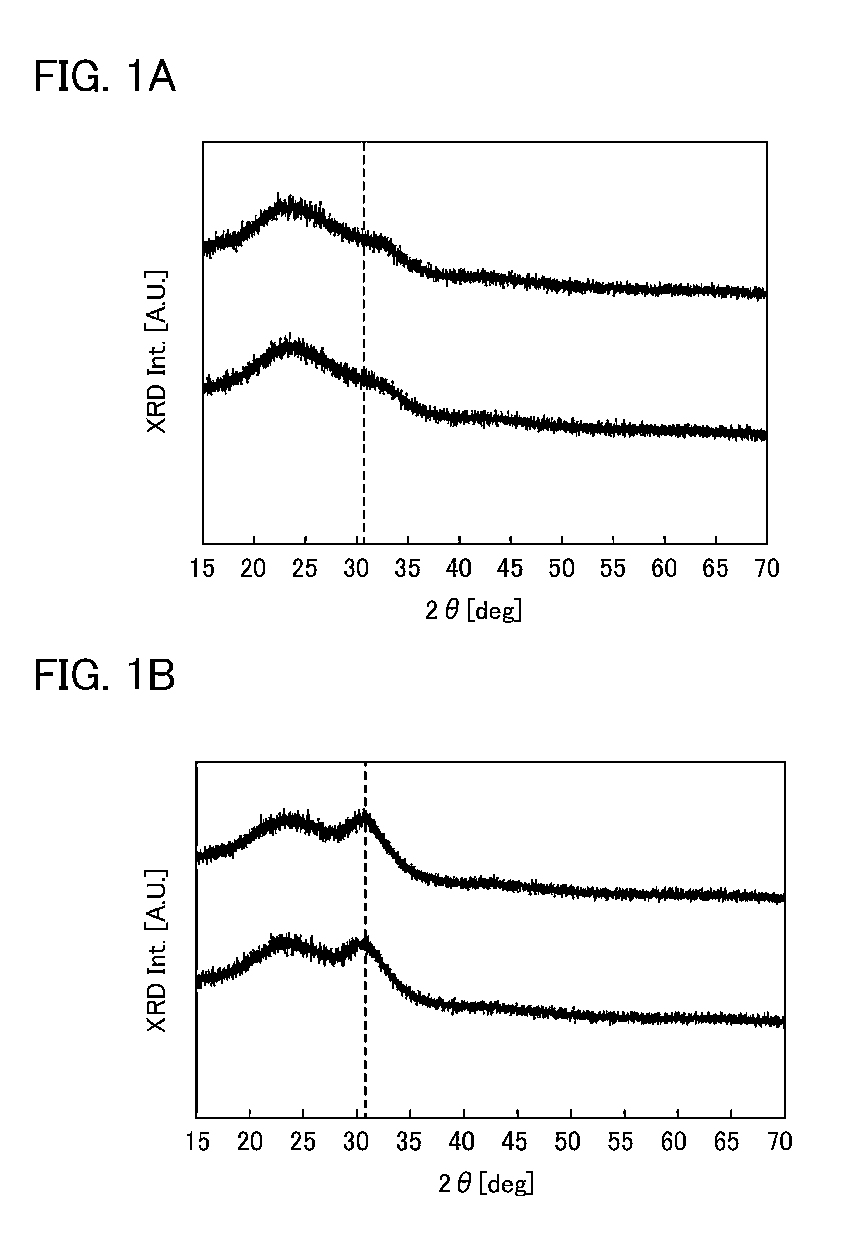
[0070]In this embodiment, the case of forming a conductive oxide film under a condition in which the percentage of an argon gas in film formation is 100% is described with reference to FIGS. 1A and 1B and Table 1.

[0071]In this embodiment, the case of forming an indium zinc oxide film is described as an example.

[0072]A method for forming the indium zinc oxide film and conditions for the film formation are described. The indium zinc oxide film was formed by a sputtering method. The conditions are described below.

[0073]A target with a composition of In:Zn=2:1 (a molar ratio of In2O3:ZnO=1:1) was used. The film formation was performed under two conditions of the substrate temperature, 200° C. and 400° C. The reaction pressure was 0.4 Pa, and the DC power was 0.5 kW.

[0074]Note that nitrogen annealing treatment was not performed after the film formation.

[0075]Table 1 shows the measurement results of the sheet resistances of the indium zinc oxide films formed under the above-de...

Example

Embodiment 2

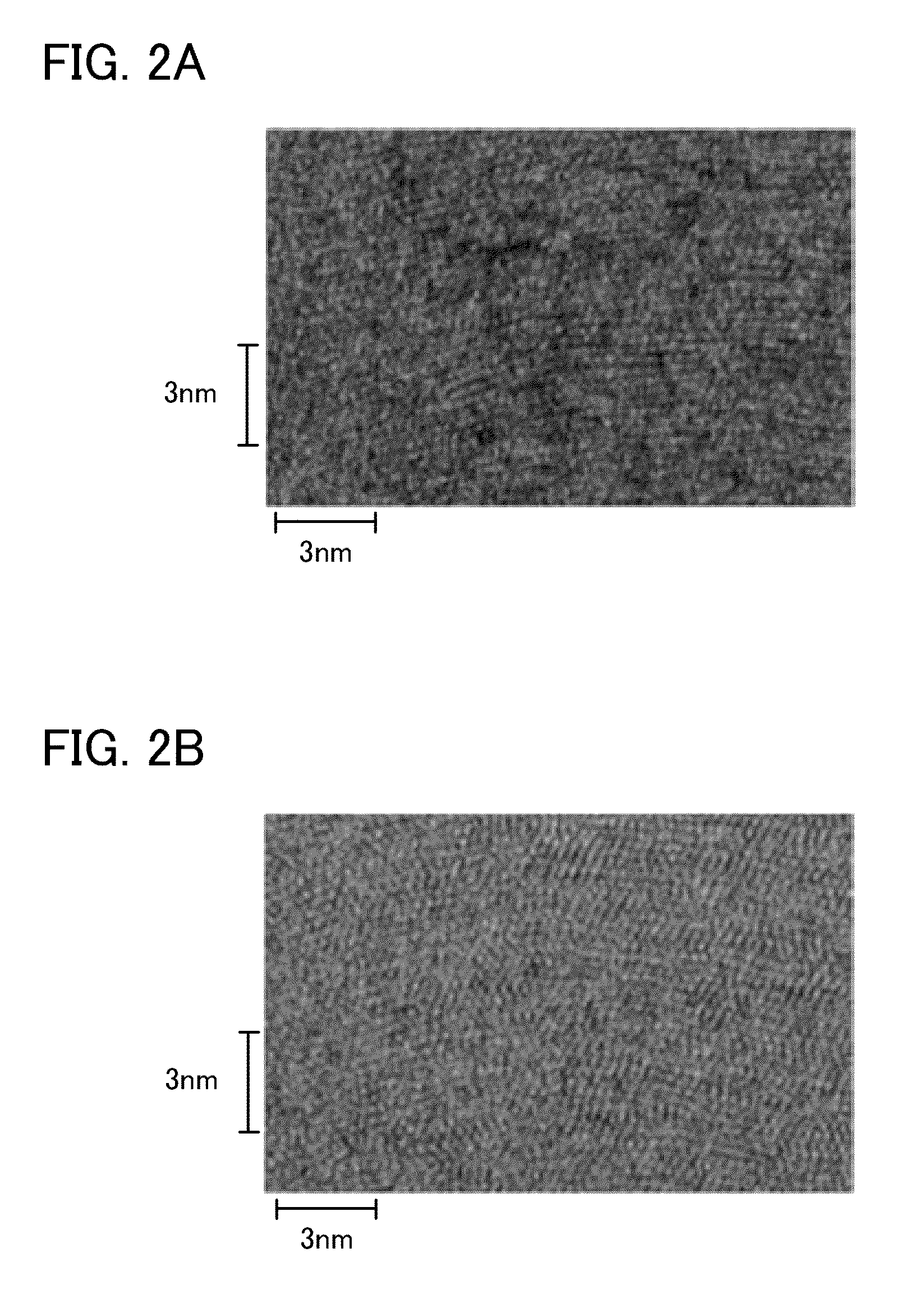
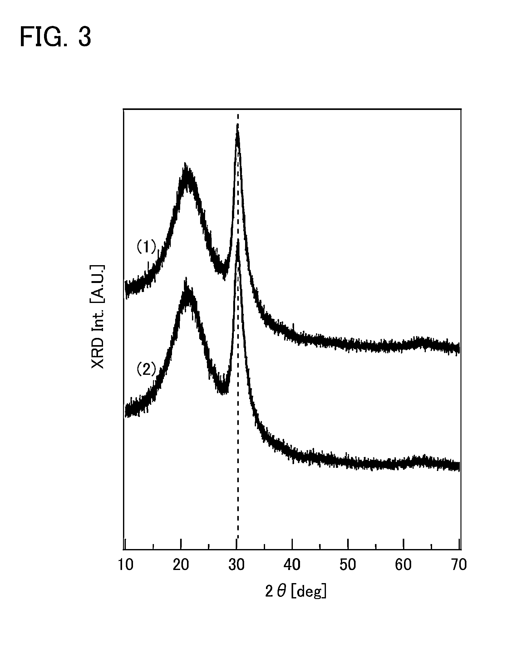
[0099]In this embodiment, the case of forming a conductive oxide film under a condition in which the percentage of an argon gas in film formation is lower than or equal to 70% is described with reference to FIGS. 2A and 2B, FIG. 3, FIG. 4, FIGS. 5A and 5B, FIG. 11, and Tables 2 to 7.

[0100]In this embodiment, the case of forming an indium zinc oxide film is described as an example.

[0101]A method for forming the indium zinc oxide film and conditions for the film formation are described. The indium zinc oxide film was formed by a sputtering method. The conditions are described below.

[0102]A target with a composition of In:Zn=2:1 (a molar ratio of In2O3:ZnO=1:1) was used. The film formation was performed under the following two conditions of the gas ratio in film formation: the percentage of an oxygen gas of 100% and the ratio of an argon gas:an oxygen gas=7:3. The film formation was performed under two conditions of the substrate temperature, 25° C. (room temperature) and 2...

Example

Embodiment 3

[0157]In this embodiment, an example of using the conductive oxide film of one embodiment of the present invention in an organic EL display device having a touch panel is described with reference to FIGS. 6A and 6B and FIGS. 7A and 7B.

[0158]As an example, an analog resistive touch panel is described with reference to FIGS. 6A and 6B.

[0159]FIG. 6A is a cross-sectional view of an organic EL display device 100 having a touch panel 20, and FIG. 6B illustrates the placement of conductive oxide films in the touch panel 20.

[0160]The organic EL display device 100 includes an organic EL display panel 10 and a touch panel 20. Although the organic EL display panel 10 and the touch panel 20 are directly bonded with an adhesive layer 300 provided therebetween in FIG. 6A, another structure may be employed. Part of the organic EL display panel 10 may be bonded to part of the touch panel 20 with an adhesive layer.

[0161]As illustrated in FIG. 6A, the touch panel 20 includes a first subst...


PUM

PropertyMeasurementUnit
Temperatureaaaaaaaaaa
Fractionaaaaaaaaaa

Abstract

One embodiment of the present invention provides a conductive oxide film having high conductivity and high transmittance of visible light. The conductive oxide film having high conductivity and high transmittance of visible light can be obtained by forming a conductive oxide film at a high substrate temperature in the film formation and subjecting the conductive oxide film to nitrogen annealing treatment. The conductive oxide film has a crystal structure in which c-axes are aligned in a direction perpendicular to a surface of the film.

Description

BACKGROUND OF THE INVENTION[0001]1. Field of the Invention[0002]The present invention relates to a conductive oxide film, a display device, and a method for forming a conductive oxide film.[0003]The present invention relates to a conductive oxide film having a crystal structure in which c-axes are aligned in a direction perpendicular to a surface of the film, and a method for forming the conductive oxide film. In addition, the present invention relates to a display device using such a conductive oxide film.[0004]2. Description of the Related Art[0005]Recently, touch panels having a multi-touch function have widespread rapidly in accordance with the increasing demand for smartphones or tablet PCs. Transparent conductive oxide films are utilized in touch panels, thin-film solar cells, and particle moving type electronic paper using electronic liquid powder. The demand for high-quality transparent conductive oxide films is expected to increase, and the market of the films will expand i...

Claims


Application Information

Patent Timeline
IPC IPC(8): G02F1/1333
CPCG02F1/13338G06F3/045G06F2203/04103G06F3/0445G06F3/0446G06F3/04166G06F3/0444G06F3/041G06F3/0412H01B5/14H01B13/00Y02E10/50H10K50/805H10K71/00H10K71/60C23C14/086C23C14/34C23C14/5806G02F1/13306G02F2201/121G02F2201/123G06F2203/04104
Inventor YAMAZAKI, SHUNPEIOOTA, MASASHI
Owner SEMICON ENERGY LAB CO LTD
Why Eureka
Try Eureka