Electrical contact element

Inactive Publication Date: 2014-05-22
VEIGEL ANDREAS
0 Cites 6 Cited by

AI-Extracted Technical Summary

Problems solved by technology

Furthermore, it should be taken into account that subassemblies or pieces of equipment often have to be arranged so as to be spatially separate from each other and in many cases, the connection technologies and solutions used then become limited in technological and economic terms.
For example, rigid printed circuit boards already cannot be used universally due to their geometry.
In the case of motor vehicle lights or fittings, for example, which are often designed to have complex and curved geometric shapes and in different planes, printed circuit boards can only be used in limited cases or can no longer be used at all.
Furthermore, an additional component support is required since a further problem which arises is the spatial positioning or mechanical arrangement of the electrical components.
Subsequent or later changes in the product development cannot be managed flexibly and lead to high tool costs.
The drawback here is that the contact surfaces, in...

Abstract

Electrical contact element for mechanical introduction into an accommodating opening, provided therefor, in a component mount, which electrical contact element has a contact part wound from electrically conductive connecting wire, which contact part comprises at least two complete wire turns so as to form a substantially cylindrical contact accommodating area which is open on both sides, for accommodating an electrical connection pin of a component to be connected to the contact element, said connection pin having a plurality of outer edges provided for contact-making.

Application Domain

Coupling contact membersConnections effected by permanent deformation

Technology Topic

Electrically conductiveElectricity +4

Image

  • Electrical contact element
  • Electrical contact element
  • Electrical contact element

Examples

  • Experimental program(1)

Example

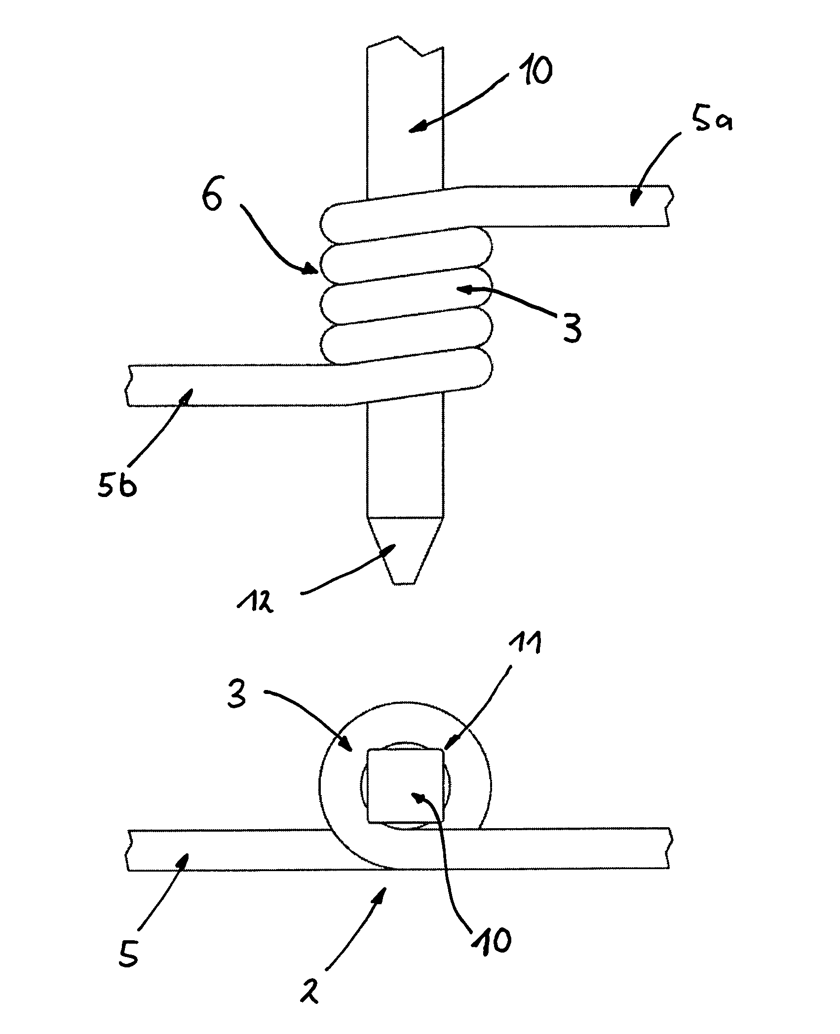
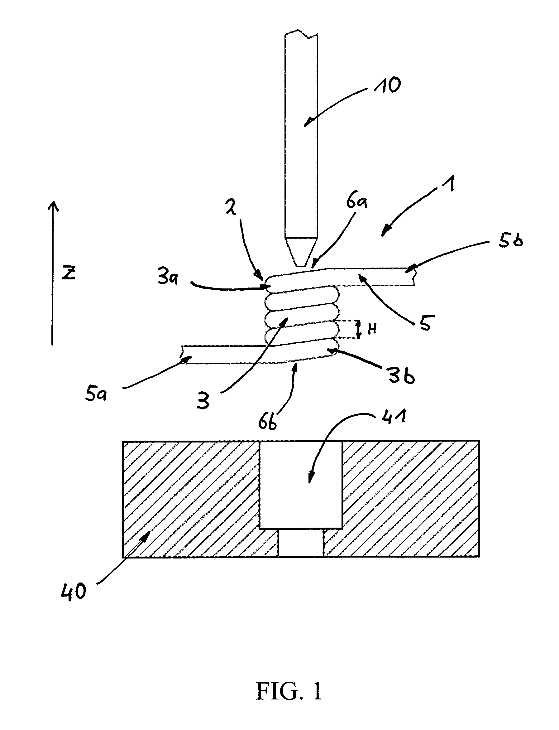
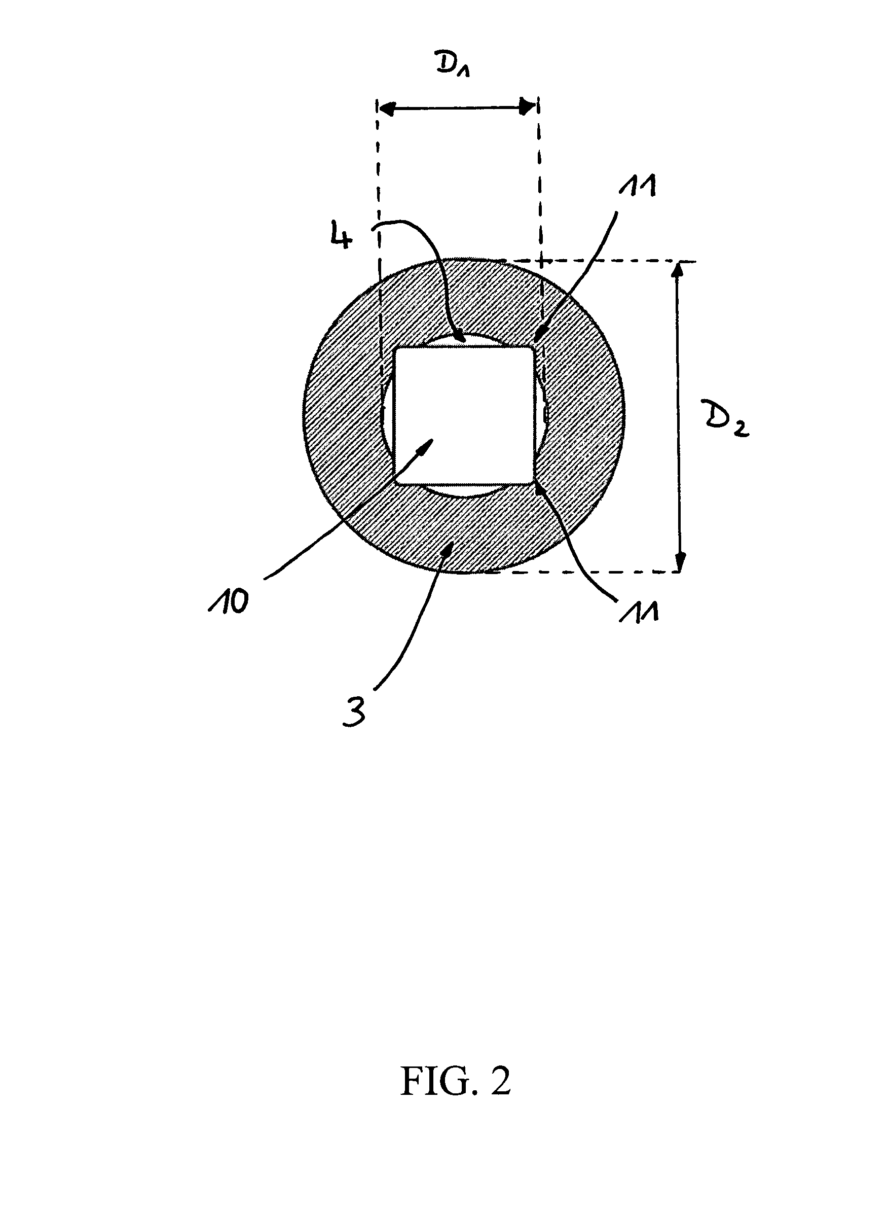
[0032]FIG. 1 is a side view of a first embodiment of a contact element 1 having a connector pin 10 arranged thereabove in the unconnected state above a component support 40 having a receiving opening 41. The contact element 1 has a contact part 2 wound from wire 5, which contact part forms a substantially cylindrical contact-receiving space 4 which is open on both sides. The contact-receiving space 4 therefore has an upper opening 6a and a lower opening 6b which are formed and limited by the uppermost and lowermost turn of wire 3a, 3b respectively.
[0033]The present embodiment shows a contact part 2 wound from four complete turns of wire 3, 3a, 3b, which contact part is wound helically from wire. The contact part 2 has a pitch H, the pitch H representing the distance by which the helix winds upwards (in the cylinder axis direction Z) in one complete rotation of the wire 5. If the pitch H corresponds to the wire diameter DWIRE, each two adjacent turns of wire 3, 3a, 3b, as shown in FIGS. 1 and 3, rest on each other and form a contact-receiving space 4 which is closed by the wire casing 6 in the casing region. Here, one complete turn of wire 3, 3a, 3b is understood to be when the wire is wound about 360°, as described previously.
[0034]As shown in a rudimentary manner in FIGS. 1 and 3, the wire pieces 5a, 5b can lead to adjacent contact parts 2 or can be produced as one piece therewith and connected thereto. This also allows contact elements 1 to be freely introduced into component supports, which are spatially separated from each other, in the space and thus, if appropriate, by the wire 5 being deflected and bent multiple times at the points, provided therefor, in component supports 40.
[0035]A connector pin 10 which is suitable for the contact-receiving space 4 of the contact part 2 is further shown in FIG. 1. The connector pin 10 is advantageously designed to have a tapered pin tip 12. FIG. 2 shows an exemplary view of a turn of wire 3 of the contact part 2 of a contact element 1 with a connector pin 10 having a square cross section arranged thereabove.
[0036]The contact-receiving space 4 of the contact element 2 has a substantially circular cross section having an inner diameter D1. The connector pin 10 shown here has four outer edges 11 extending in the plugging direction, which edges are also denoted as contact edges 11 in the following. The outer dimension of the connector pin 10, that is to say the distance between two opposite contact edges 11, is designed to be slightly larger than the inner diameter D1 of the contact-receiving space 4. When an in particular solid connector pin 10 is introduced, as shown in FIG. 3, the contact edges 11 are materially deformed and/or cold-welded to the contact points of the contact element 2 which creates a gas-tight connection between the outer edges 11 of the pin and the connection points in the contact element 2.
[0037]The outer edges 11 of the pin, which are provided for contacting, preferably extend over the entire height of the contact-receiving space 4 of the contact part 2 and are provided with radii, as can be seen in FIG. 2. In the connected state, each turn of wire 3, 3a, 3b is thus contacted by the contact edges 11. The contact part 2 has an outer diameter D2. Changing the diameter of the wire DWIRE and the inner diameter D1 of the contact element 2 makes it possible to form a plurality of different contact elements 1.
[0038]FIG. 4 shows a contact assembly 50 consisting of two interconnected contact elements 1 made from a common wire 5. According to the invention, contact assemblies 50 can also be formed in a complex manner and can for example also be formed from insulated wire.
[0039]FIG. 5 shows a further embodiment of a connection arrangement according to the invention between a contact element and a further connector pin shape according to the invention which corresponds thereto. It can be seen here that the outer edges of the specially shaped connector pin penetrate the insulating casing of the contact element 1.
List of Reference Signs
[0040] 1 Contact element [0041] 2 Contact part wound from wire [0042] 3 Turns of wire [0043] 3a, b Upper and lower turn of wire [0044] 4 Contact-receiving space [0045] 5 Wire [0046] 5a, b Wire pieces [0047] 6 Wire casing [0048] 6a, 6b Upper and lower opening [0049] 10 Connector pin [0050] 11 Outer edges (contact edges) [0051] 12 Pin tip [0052] 20 Component [0053] 30 Connection wire [0054] 40 Component support [0055] 41 Receiving opening [0056] 50 Contact arrangement [0057] D1 Inner diameter [0058] D2 Outer diameter [0059] DWIRE Diameter of the wire [0060] H Pitch [0061] Z Cylinder axis

PUM

no PUM

Description & Claims & Application Information

We can also present the details of the Description, Claims and Application information to help users get a comprehensive understanding of the technical details of the patent, such as background art, summary of invention, brief description of drawings, description of embodiments, and other original content. On the other hand, users can also determine the specific scope of protection of the technology through the list of claims; as well as understand the changes in the life cycle of the technology with the presentation of the patent timeline. Login to view more.
Why Eureka
Try Eureka