Switching power source device
- Summary
- Abstract
- Description
- Claims
- Application Information
AI Technical Summary
Benefits of technology
Problems solved by technology
Method used
Image

Examples
Example
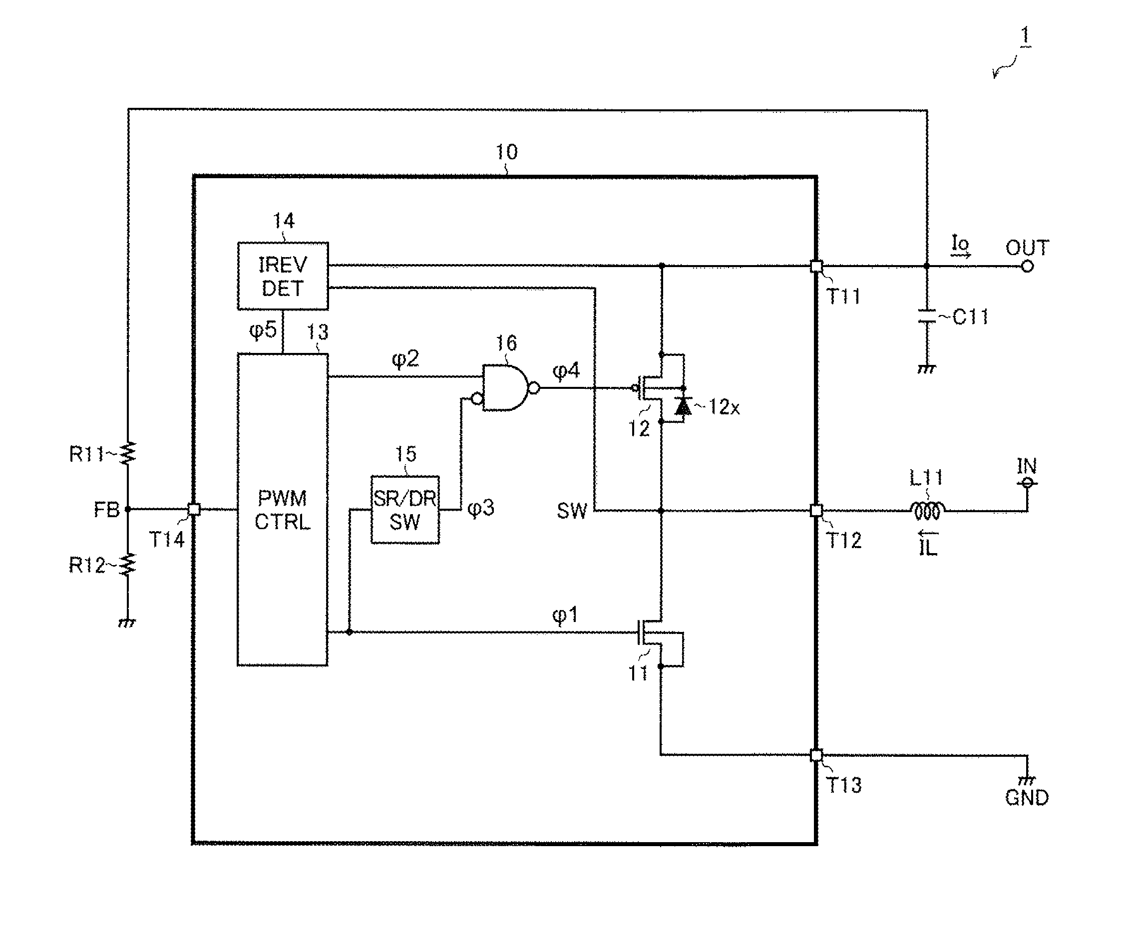
[0025]FIG. 1 is a block diagram showing a first embodiment of a switching power source device. A switching power source device 1 of the first embodiment is a switching power source device of the positive voltage step-up type based on the synchronous rectification method, which boosts an input voltage IN to generate a desired output voltage OUT and supplies the output voltage OUT to an unshown load (for example, a liquid crystal display panel). The switching power source device 1 has a semiconductor device 10 and various discrete components (an inductor L11, a capacitor C11, and resistors R11 and R12) externally connected to the semiconductor device 10.
[0026]The semiconductor device 10 has external terminals T11 to T14 for establishing an electrical connection with the outside. Outside the semiconductor device 10, the external terminal T11 (output terminal) is connected to an application end of the output voltage OUT and to each of a first end of the capacitor C11 and a first end of ...
Example
Second Embodiment
[0077]FIG. 7 is a block diagram showing a second embodiment of the switching power source device. The second embodiment is fundamentally similar in configuration to the first embodiment and is characterized in that a Schottky barrier diode SBD is externally connected between the external terminals T11 and T12. Constituent components similar to those in the first embodiment, therefore, are denoted by the same reference characters as in FIG. 1, with duplicate descriptions thereof omitted, and the following focuses on characteristic features of the second embodiment.
[0078]As described above, in a switching power source device 1 of the second embodiment, the Schottky barrier diode SBD is connected in parallel with a synchronous rectification transistor 12. While a body diode 12x has a forward drop voltage of 0.6 V to 0.7 V, the Schottky barrier diode SBD has a fairly low forward drop voltage of 0.1 V to 0.2 V. Consequently, compared with the first embodiment in which th...
Example
Third Embodiment
[0079]FIG. 8 is a block diagram showing a third embodiment of the switching power source device. The third embodiment is fundamentally similar in configuration to the first embodiment and is characterized in that an input blocking transistor 17 that connects / disconnects a supply path of an input voltage IN is provided. Constituent components similar to those in the first embodiment, therefore, are denoted by the same reference characters as in FIG. 1, with duplicate descriptions thereof omitted, and the following focuses on characteristic features of the third embodiment.
[0080]The input blocking transistor 17 is a switch element (P-channel type MOS field-effect transistor) having a polarity opposite to that of a synchronous rectification transistor 12, which is inserted between an external terminal T11 and an external terminal T12 and turned on / off in accordance with a standby signal φ6. To be specific in terms of connection relationships regarding the input blocking...
PUM
 Abstract
Description
Claims
Application Information
 - R&D Engineer
- R&D Manager
- IP Professional
- Industry Leading Data Capabilities
- Powerful AI technology
- Patent DNA Extraction
Browse by: Latest US Patents, China's latest patents, Technical Efficacy Thesaurus, Application Domain, Technology Topic.
© 2024 PatSnap. All rights reserved.Legal|Privacy policy|Modern Slavery Act Transparency Statement|Sitemap