Package structures including discrete antennas assembled on a device

a technology of discrete antennas and packaging structures, which is applied in the direction of resonant antennas, substantially flat resonant elements, and particular array feeding systems, etc., can solve the problems of routing losses and loss of package real estate associated with traditional/prior art in package substrate/antenna array designs of devices using wireless debug ports

Active Publication Date: 2014-06-26
INTEL CORP
View PDF3 Cites 26 Cited by
  • Summary
  • Abstract
  • Description
  • Claims
  • Application Information

AI Technical Summary

Problems solved by technology

Applications such as ultra-short range chip-to-chip communications and post silicon validation of system on a chip(SoC)/central processing unit (CPU) devices using

Method used


Image

  • Package structures including discrete antennas assembled on a device
  • Package structures including discrete antennas assembled on a device
  • Package structures including discrete antennas assembled on a device

Examples


Embodiment Construction

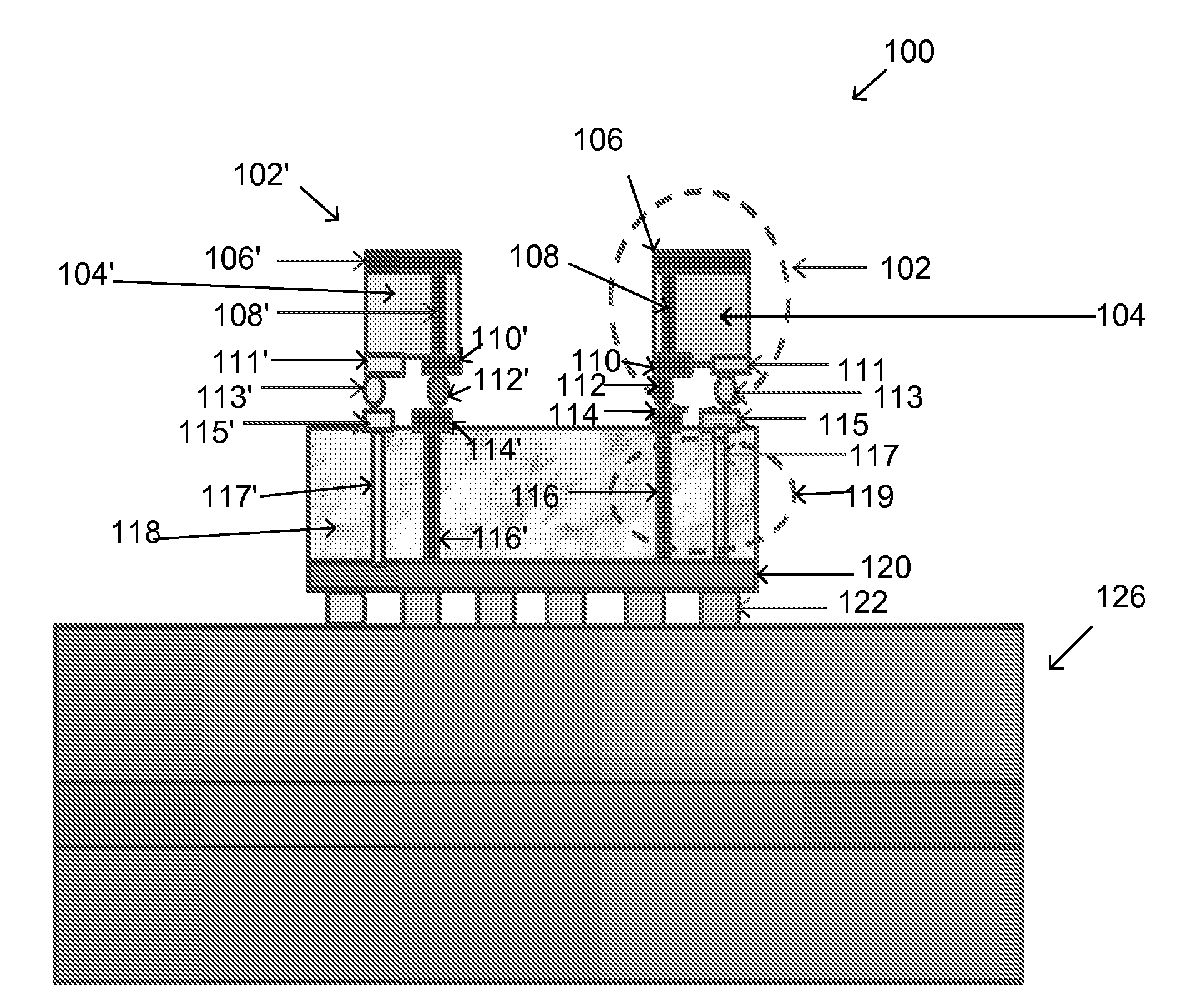
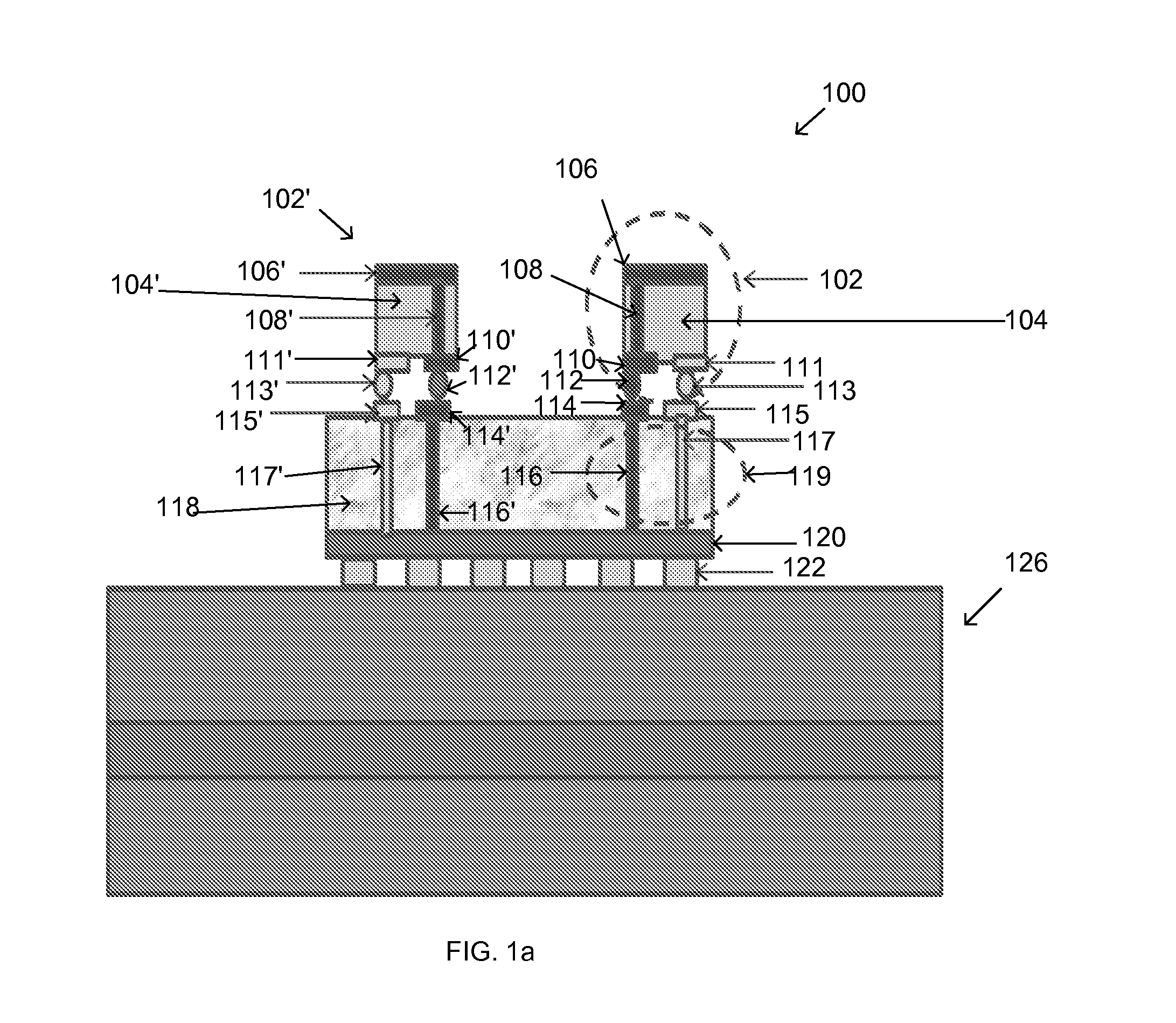
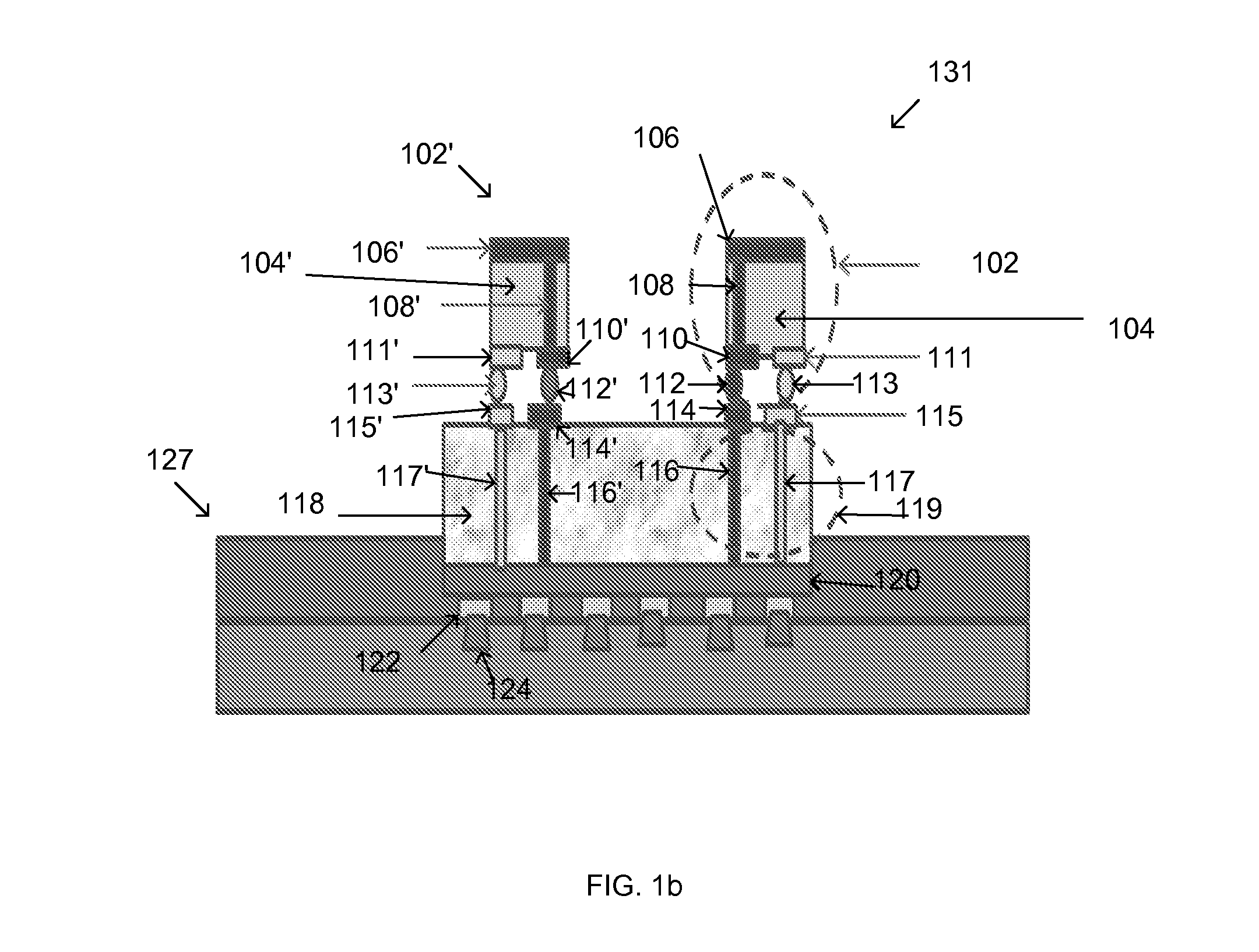
[0007]In the following detailed description, reference is made to the accompanying drawings that show, by way of illustration, specific embodiments in which the methods and structures may be practiced. These embodiments are described in sufficient detail to enable those skilled in the art to practice the embodiments. It is to be understood that the various embodiments, although different, are not necessarily mutually exclusive. For example, a particular feature, structure, or characteristic described herein, in connection with one embodiment, may be implemented within other embodiments without departing from the spirit and scope of the embodiments. In addition, it is to be understood that the location or arrangement of individual elements within each disclosed embodiment may be modified without departing from the spirit and scope of the embodiments. The following detailed description is, therefore, not to be taken in a limiting sense, and the scope of the embodiments is defined only...


PUM

PropertyMeasurementUnit
Frequencyaaaaaaaaaa
Electrical conductoraaaaaaaaaa
Waveaaaaaaaaaa

Abstract

Methods of forming a microelectronic packaging structure and associated structures formed thereby are described. Those methods and structures may include forming a package structure comprising a discrete antenna disposed on a back side of a device, wherein the discrete antenna comprises an antenna substrate, a through antenna substrate via vertically disposed through the antenna substrate. A through device substrate via that is vertically disposed within the device is coupled with the through antenna substrate via, and a package substrate is coupled with an active side of the device.

Description

BACKGROUND OF THE INVENTION[0001]The integration of millimeter wave radios operating at 30 GHz or above on platforms allows for the wireless transfer of data between devices or between chips. The successful transfer of data between the devices / chips requires one or more package-level integrated antennas that serve as an interface. Applications such as ultra-short range chip-to-chip communications and post silicon validation of system on a chip(SoC) / central processing unit (CPU) devices using wireless debug ports may suffer from routing losses and loss of package real estate associated with traditional / prior art in package substrate / antenna array designs.BRIEF DESCRIPTION OF THE DRAWINGS[0002]While the specification concludes with claims particularly pointing out and distinctly claiming certain embodiments, the advantages of these embodiments can be more readily ascertained from the following description of the invention when read in conjunction with the accompanying drawings in whic...

Claims


Application Information

Patent Timeline
IPC IPC(8): H01Q1/38H01P11/00
CPCH01L2224/16225H01L2924/15311H01Q1/2283H01Q1/38H01P11/00Y10T29/49018H01L2223/6677H01L23/481H01L23/66H01Q1/526H01Q9/045H01Q21/0006
Inventor KAMGAING, TELESPHORRAO, VALLURI R.DEGANI, OFIR
Owner INTEL CORP
Why Eureka
Try Eureka